In the previous post in this series, I wrote about several prototyping steps for this project. In this article, I am going to describe the final version.
This article is Part 3 in a 3-Part Series.
- Part 1 -Freeform ESP8266 OLED MQTT client
- Part 2 -ESP8266 based room-conditions monitor, Part 1
- Part 3 -ESP8266 based room-conditions monitor, part 2: PCB
The idea for the final form
I wanted to move from prototypes to something nicer and more final. But I still wanted to utilize those small sensor breakouts and the charging module. I already owned them (and the sensors are very small and would be difficult to solder).
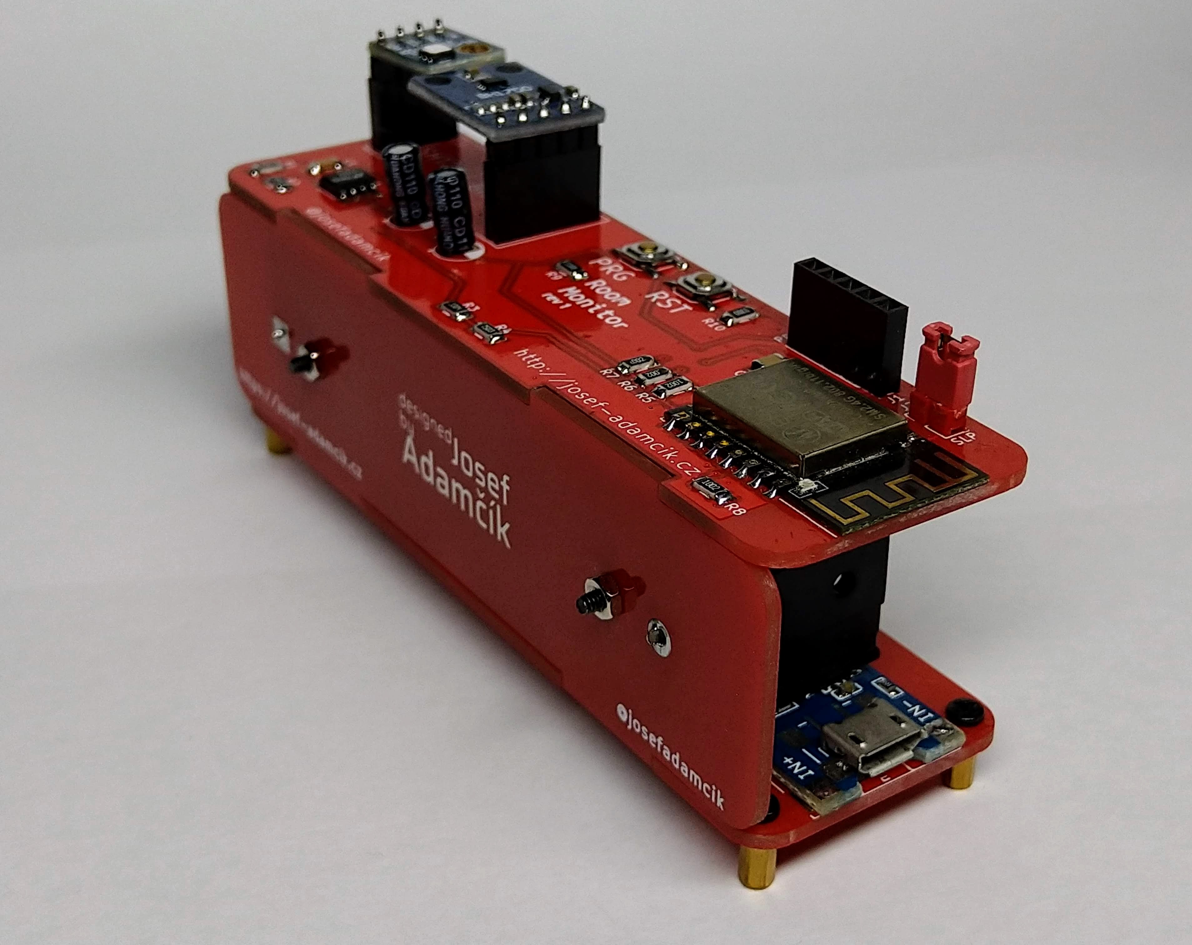
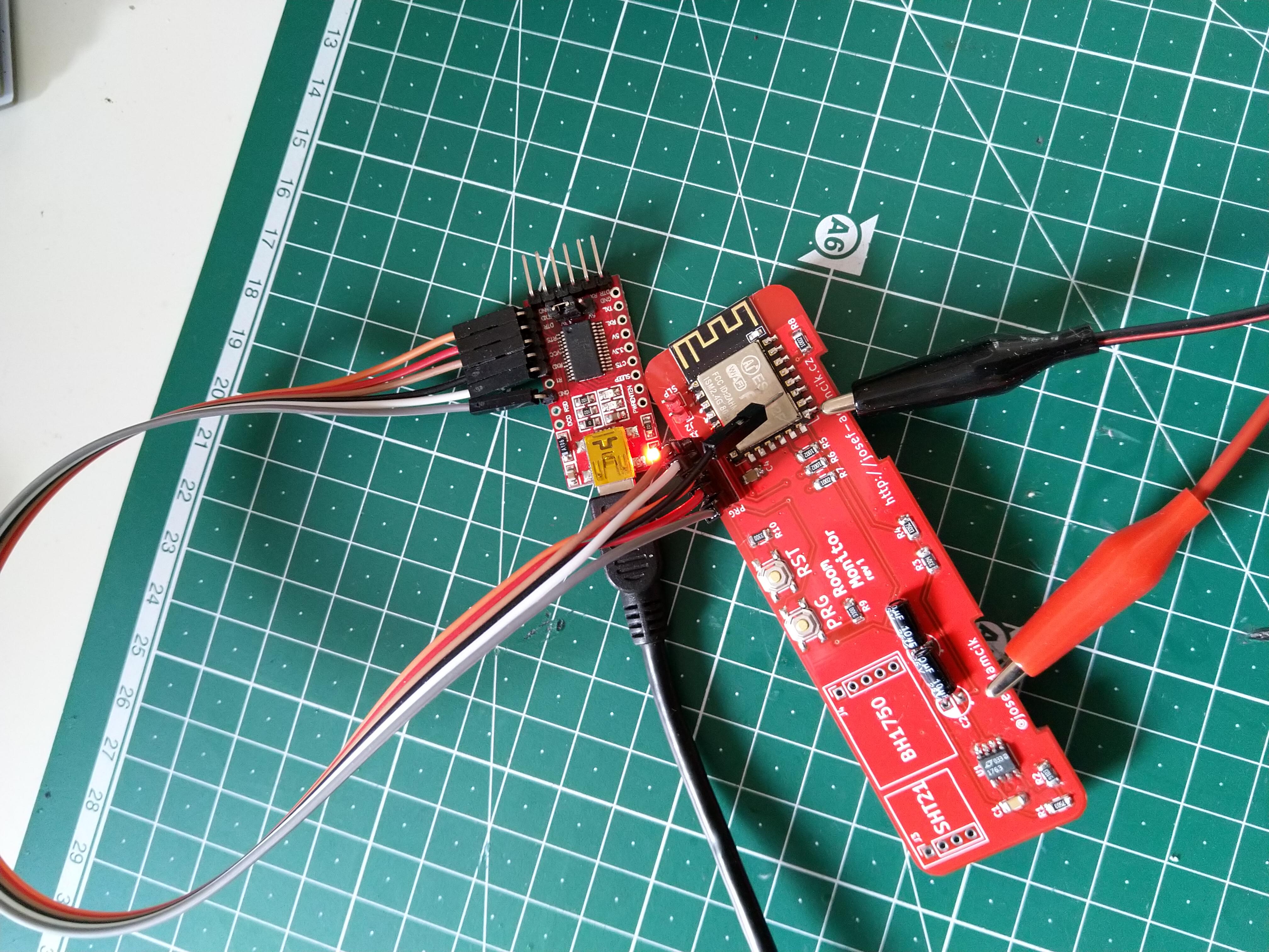
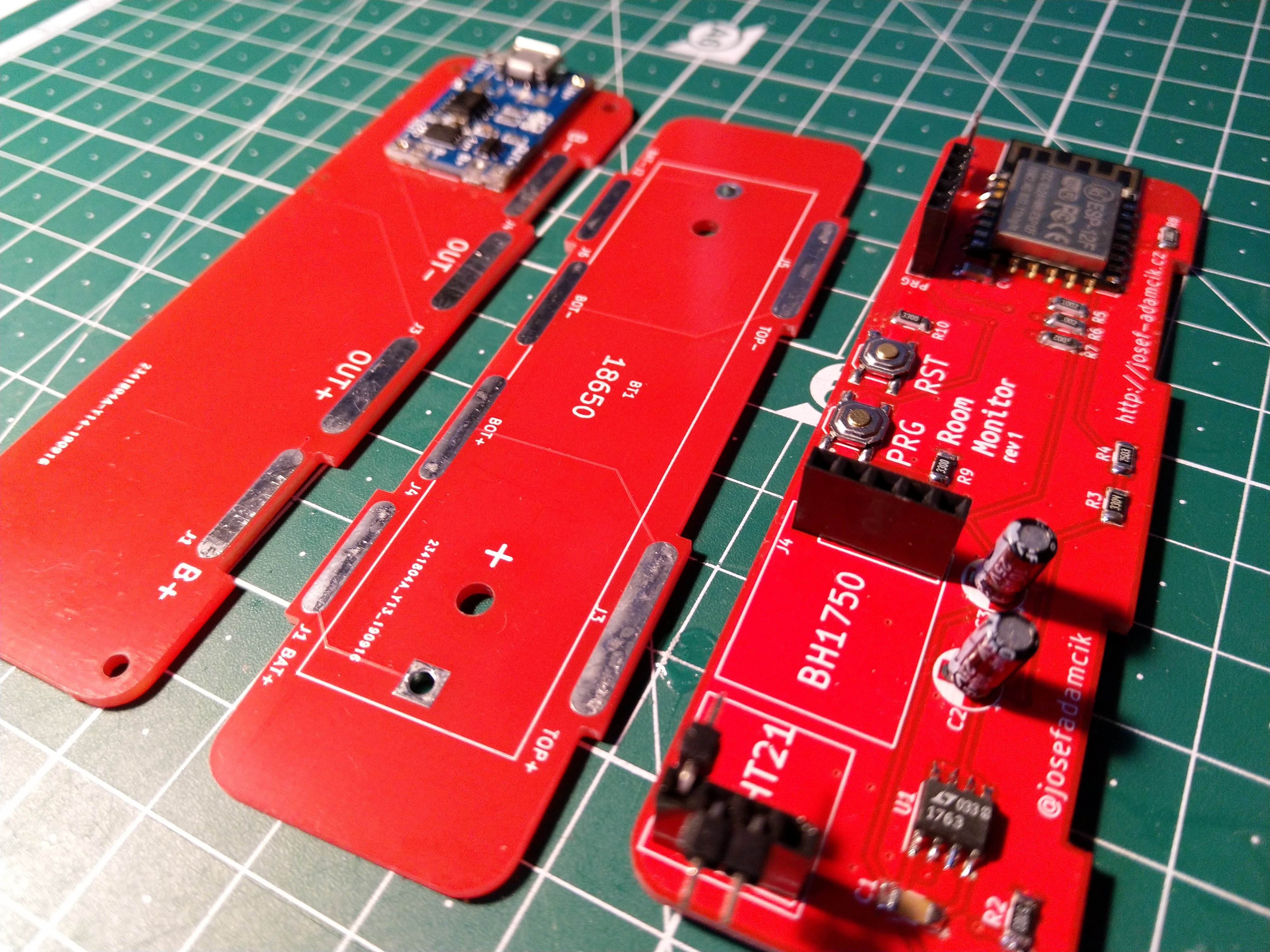
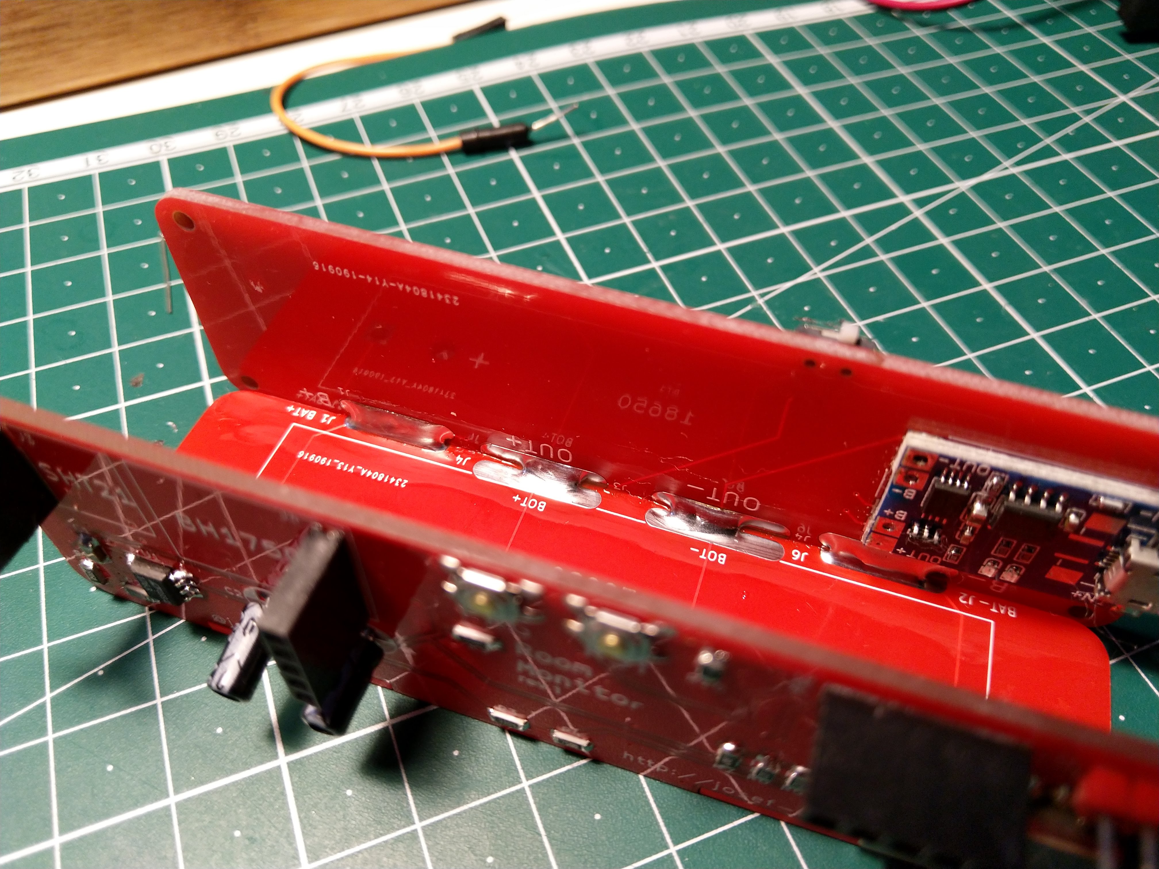
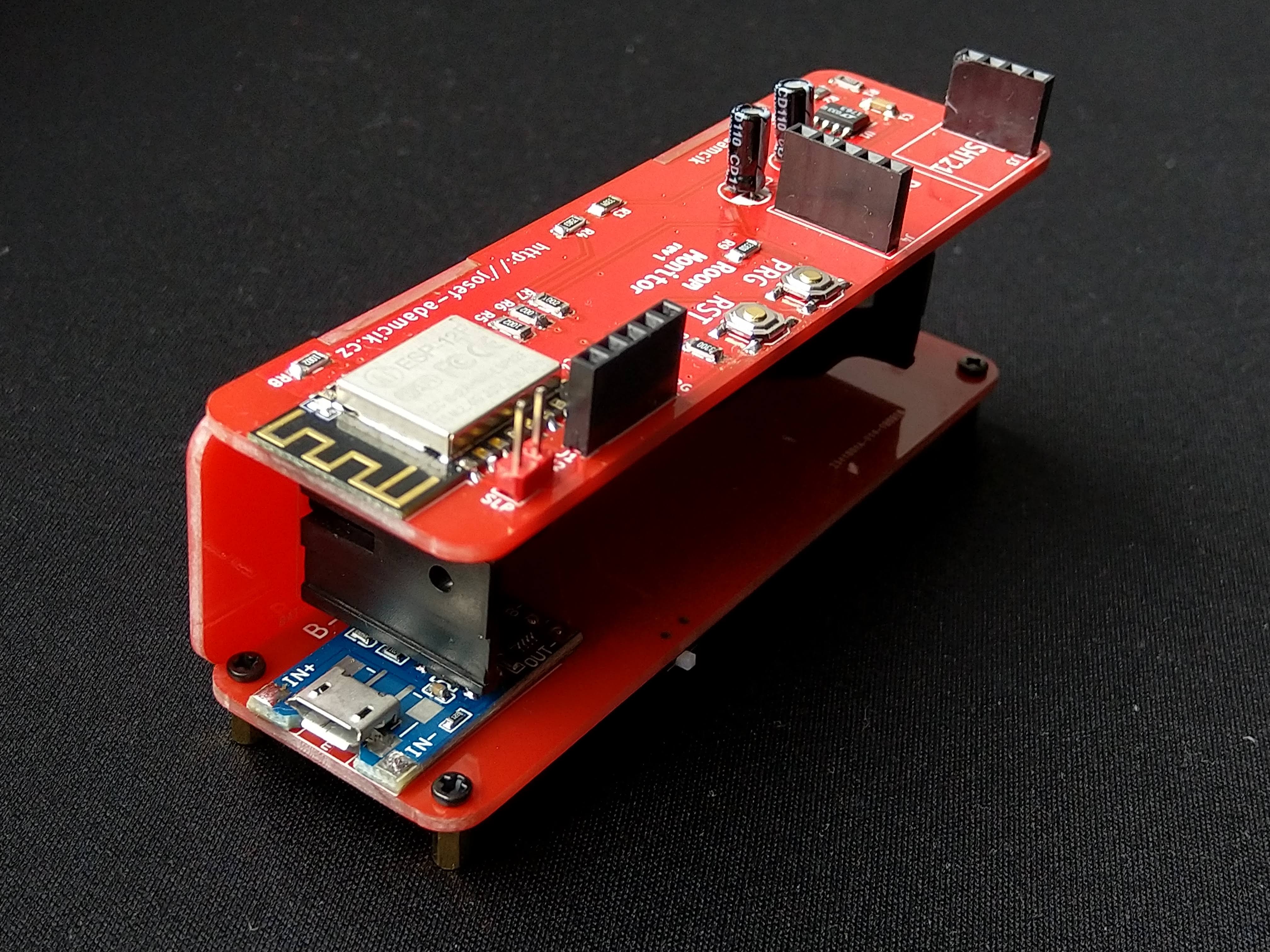
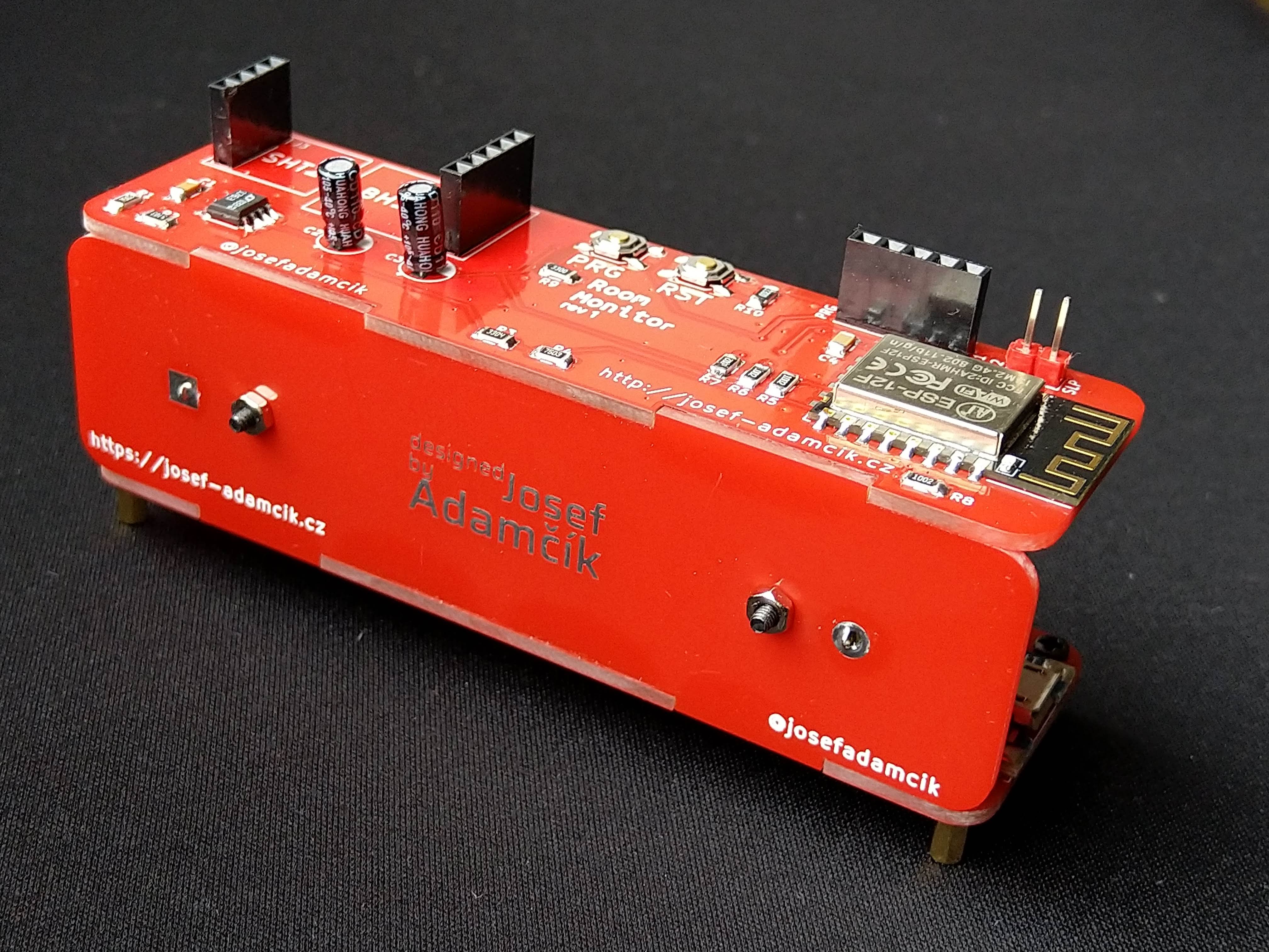
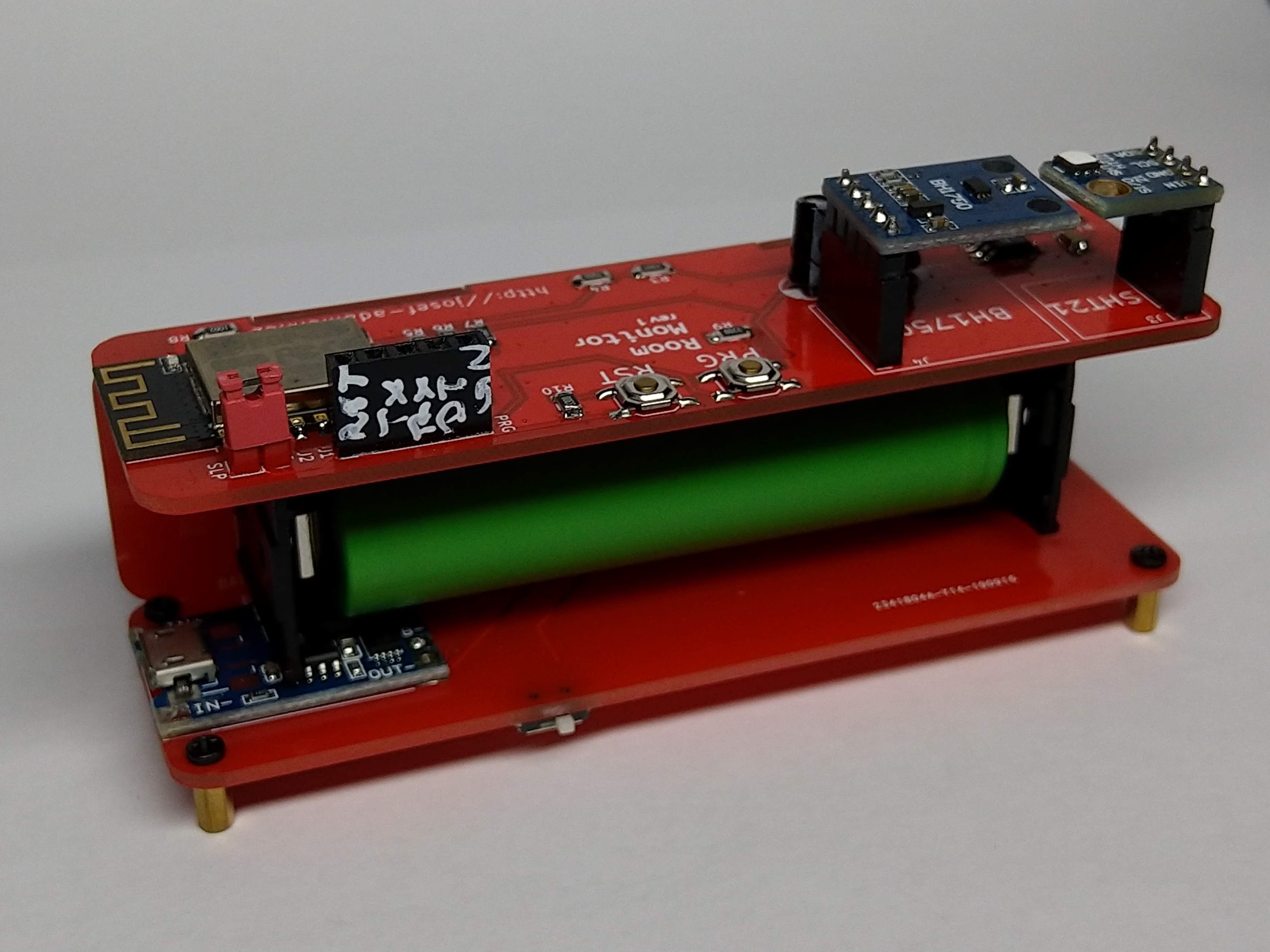
Free-forming and building something similar to the client device would be also an option and I might still do it in the future. But I also wanted to have the ability to build more copies of the device. Since I recently began to learn how to make PCBs, I thought this might be another opportunity to gather some experience. But I didn’t like the idea of having just one plain and boring PCB. So I tried to come up with something a little bit more interesting. The final design has 3 small boards soldered together to create a shell around a battery holder.
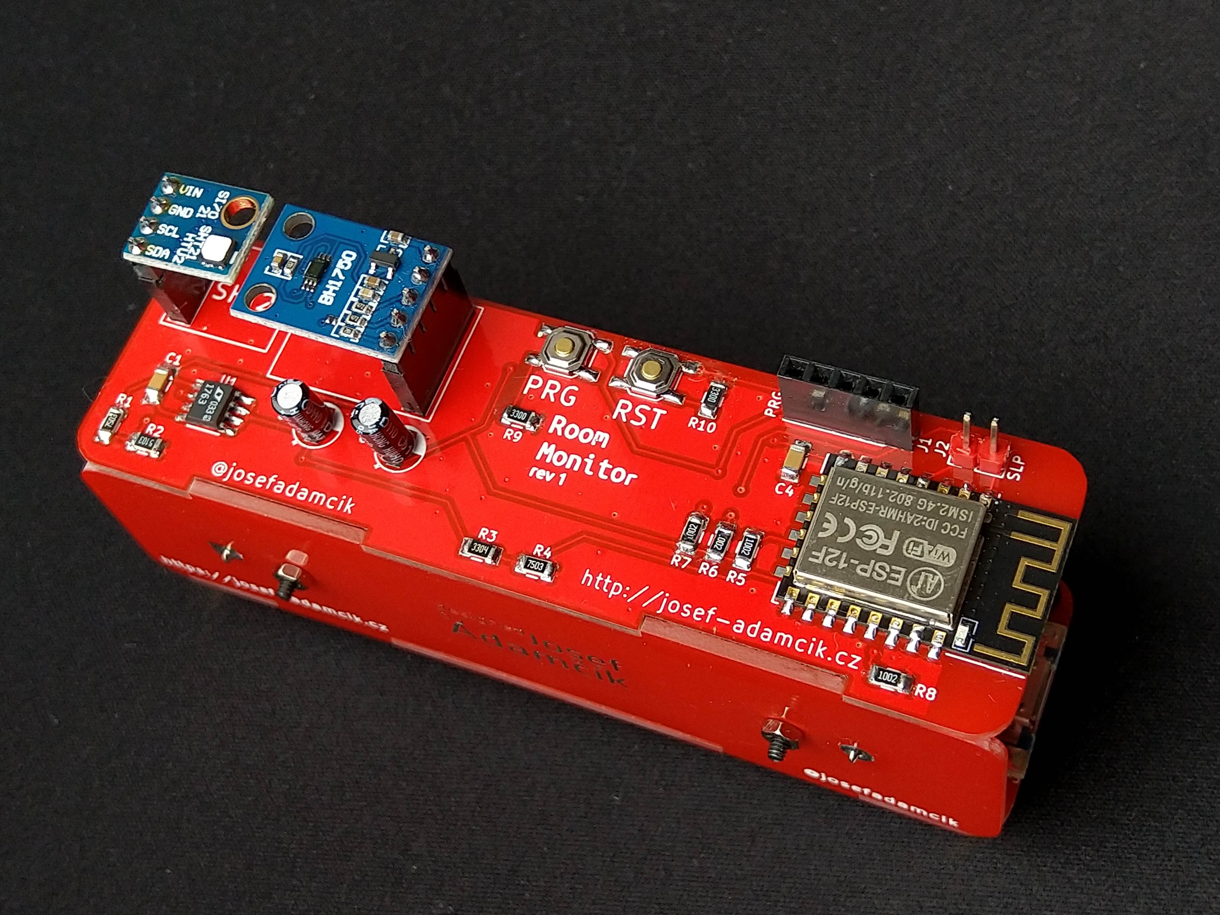
The circuit is basically the same as for the last prototype, only the components are going to be distributed across the three PCB panels.
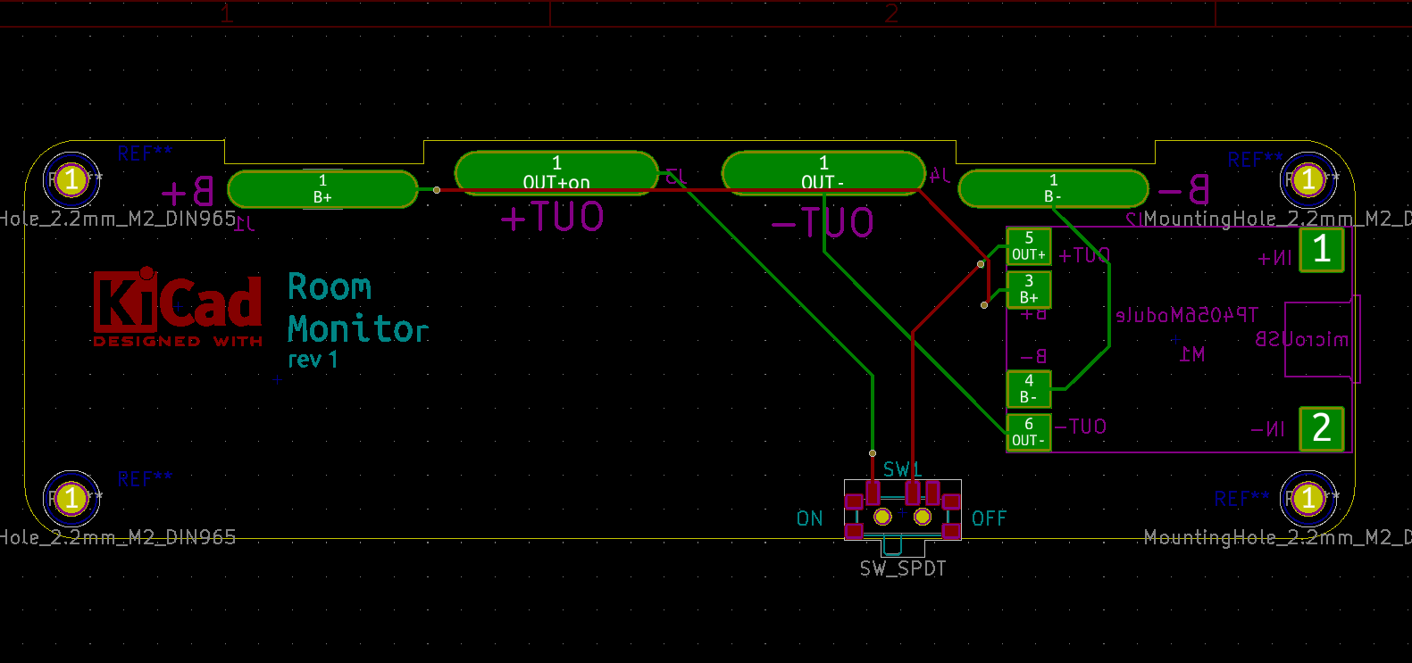
Schematic
You can find schematics for all three panels in KiCad projects on Github (there are 3 KiCad projects). I have also combined all of them in the following image.
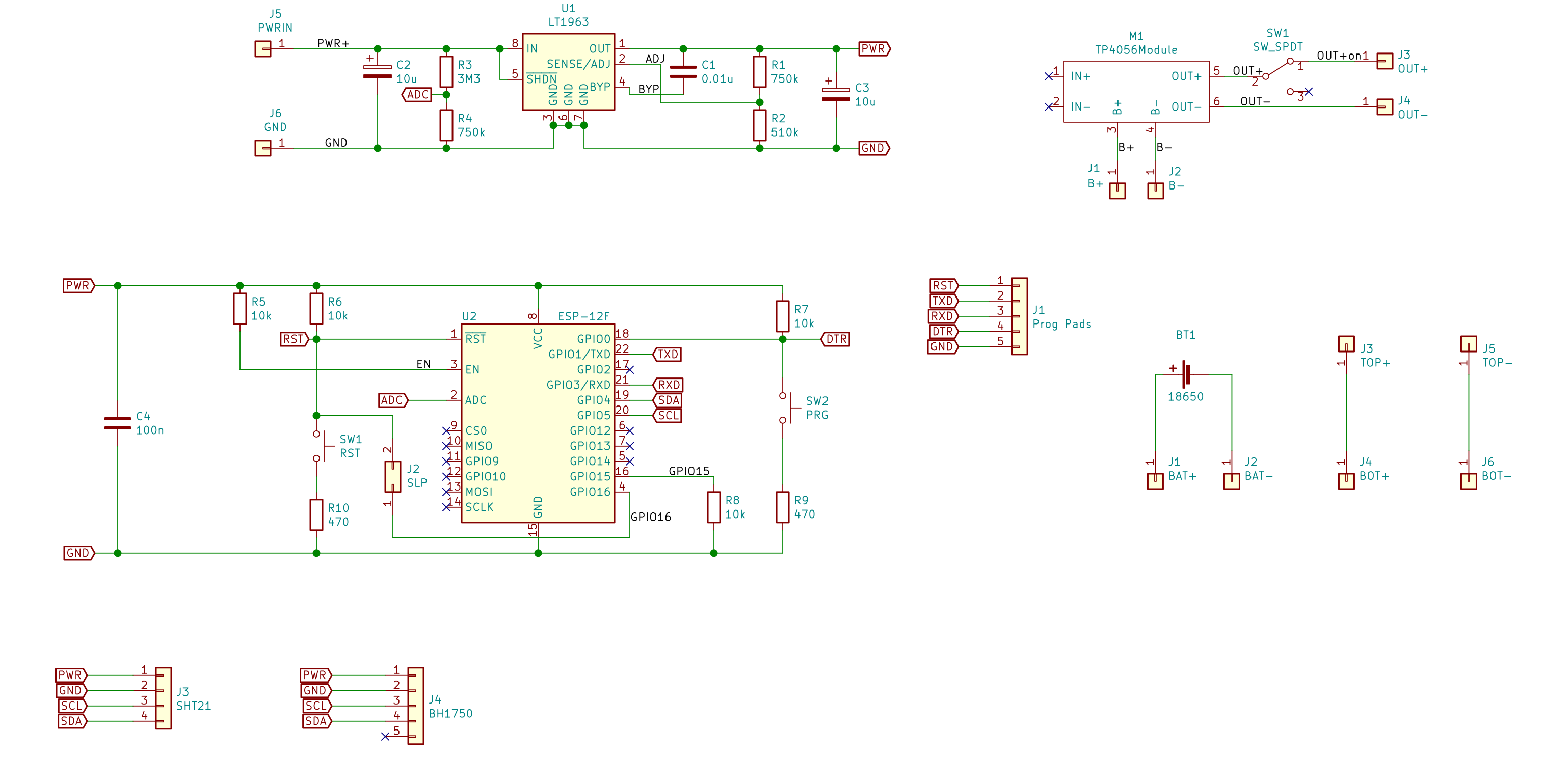
The first block (top left) is the power source with LT1763 LDO almost exactly as in the datasheet. Resistors R3 and R4 form a voltage divider for ADC in ESP8266 so that a voltage on the battery can be measured.
On the top right, the connection for the charging breakout is depicted. I decided to put the on-off switch between the module and the rest of the circuit. This allows me to turn the main circuit off during charging. But it also means that the TP4056 charging module is connected to the battery all the time.
The middle part shows connections for ESP8266. This is heavily inspired by a schematic in the documentation for Arduino core for ESP8266. Let me go through the important bits:
GPIO15is pulled down all the time,ENis pulled up.RSTis pulled up byR6, it is also connected to anRSTpin on the FTDI header.SW1allows me to restart the ESP8266 manually. And finally, the jumperJ2can be used to connectRSTtoGIPIO16which is required for deep sleep to work.GPIO0allows choosing between boot modes (UARTfor programming andFLASHfor normal operation). Normally it is pulled high (FLASH). The buttonSW2can be used to activate the programming mode (holdSW2and pressSW1). It’s also connected to theDTRpin on the FTDI header.- Serial:
RXD,TXDgoes directly to the FTDI header. - I2C:
SDA,SDLconnect ESP8266 to sensors. ADCis connected to the voltage divider mentioned above.- There are some capacitors to improve stability.
Designing the PCB
I started by creating the basic shape - a rectangle with rounded corners - in Inkscape. I created 3 copies and added notches which should allow me to fasten the panels together.
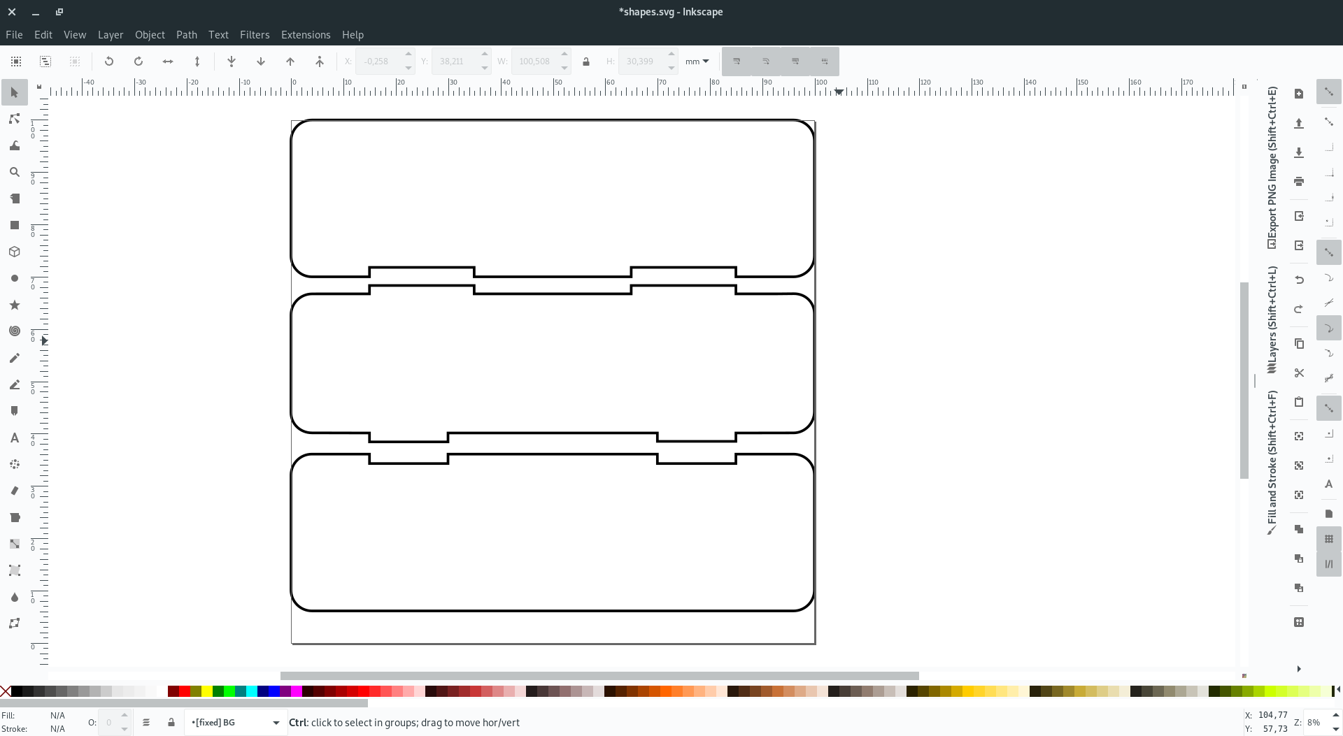
I didn’t know how to ensure they would fit each other as I wanted. I was afraid they might be either too loose or too tight. I also realized manufacturing tolerances would play a role. In the end, I decided I should start with the simplest solution and not overthink it.
I split the shapes into separate files and extracted them to DXF so they can be imported to KiCad. The basic steps are:
- Flatten the curves (
Extensions->Modify path->Flatten Beziers) - Save as DXF file
- In KiCad, choose
Import Graphicsand select the DXF file. Make sure the Edge.Cuts layer is selected as “Graphics layer”
Or you could use the SVG2Shenzen Inkscape plugin.
PCB
As I mentioned above, there are 3 PCBs, therefore 3 KiCad projects. Every project has its own schematic. I am not going to dive into the details since everything should be quite straight forward if you are familiar with KiCad. If not, there are plenty of tutorials online to learn it.
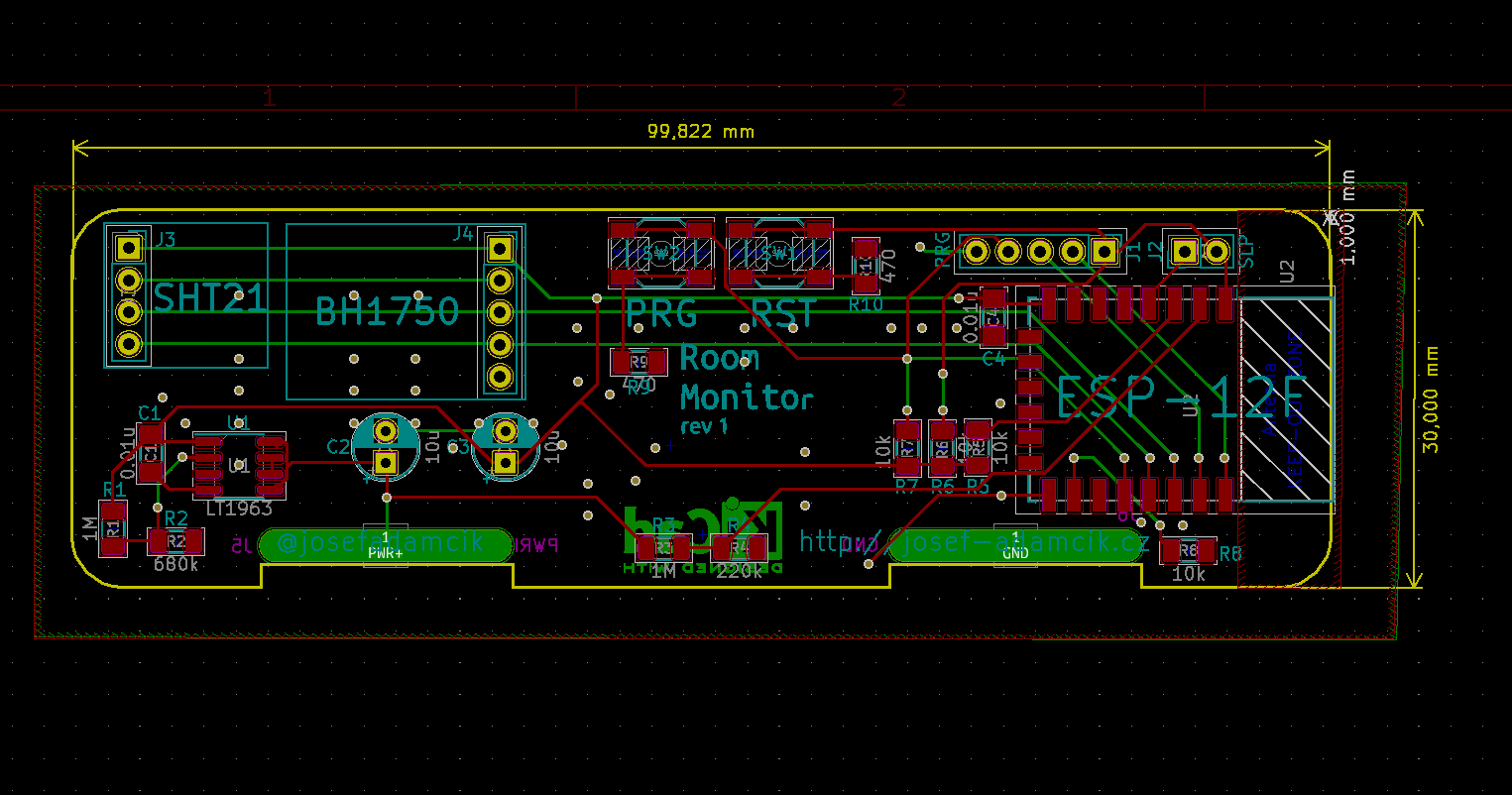
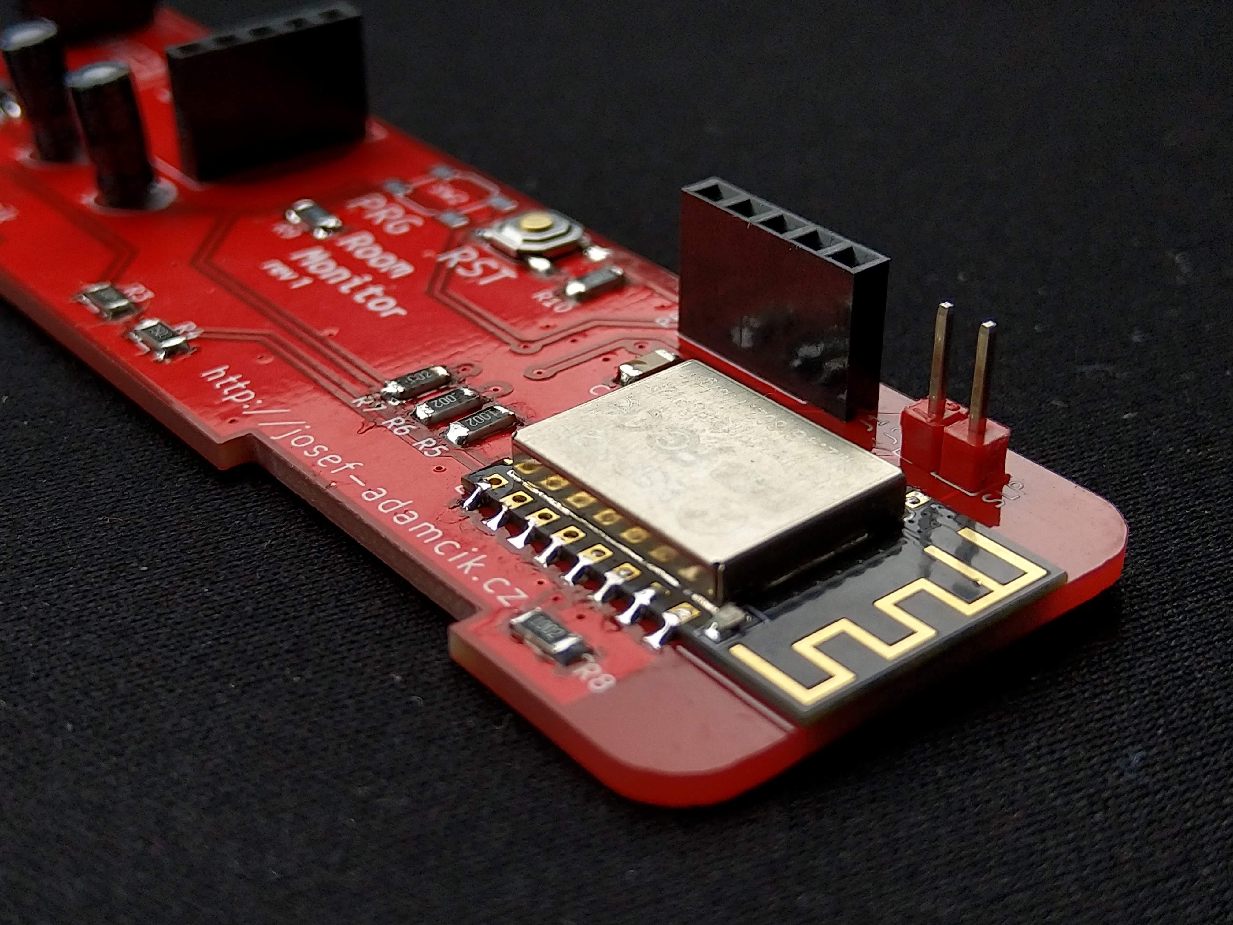
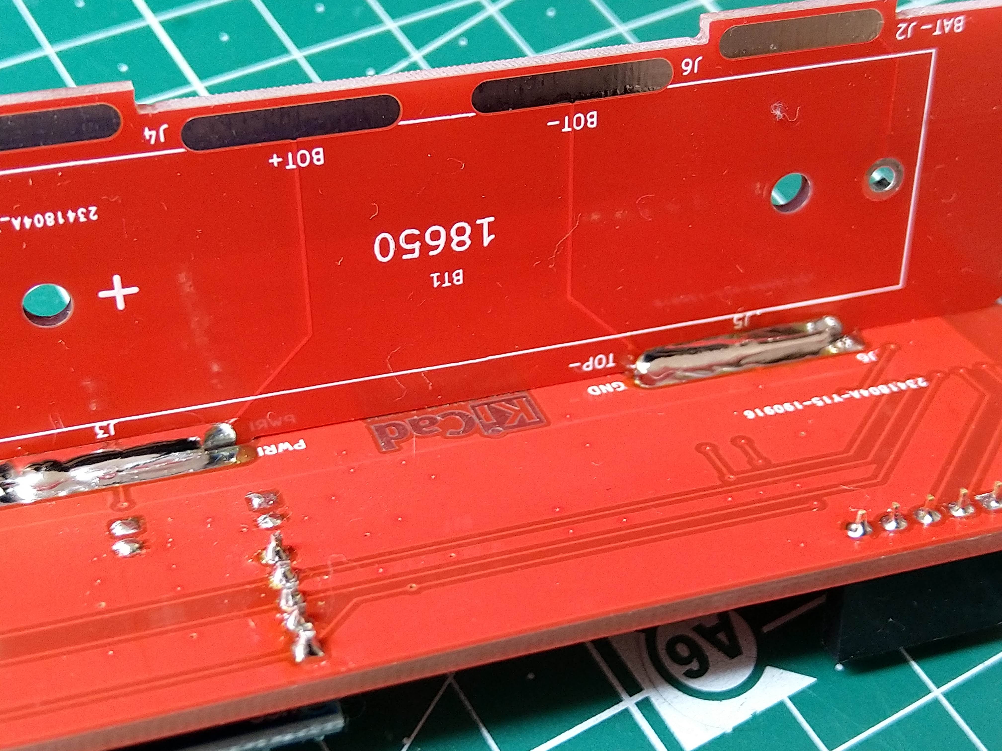
The wide pads on all the boards are where the connections between individual boards are going to be made. The idea is to use a generous amount of solder to connect boards together and create an electrical and structural connection. Of course, a regular solder is used so the mechanical connection is not going to be perfect.
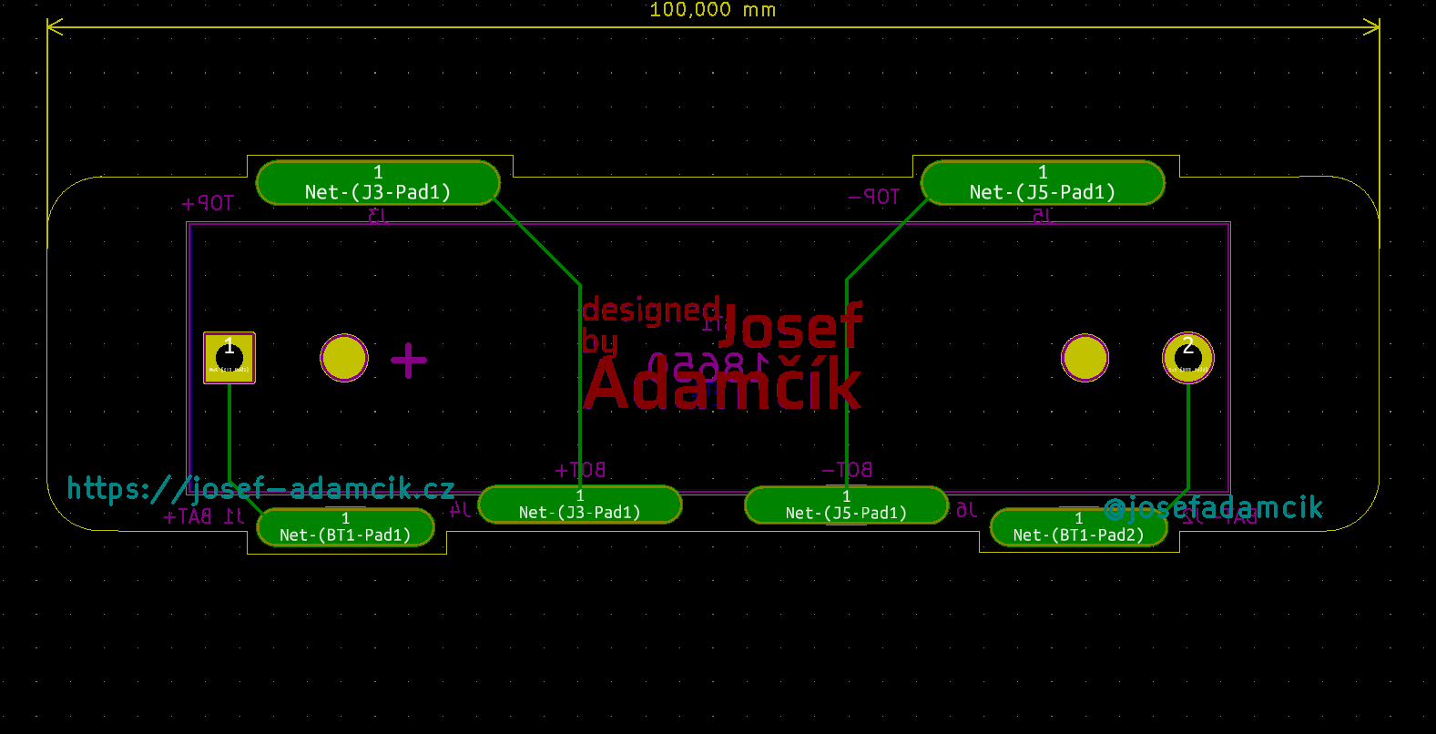
The holes in the corners of the bottom PCB are for legs made from brass standoffs.
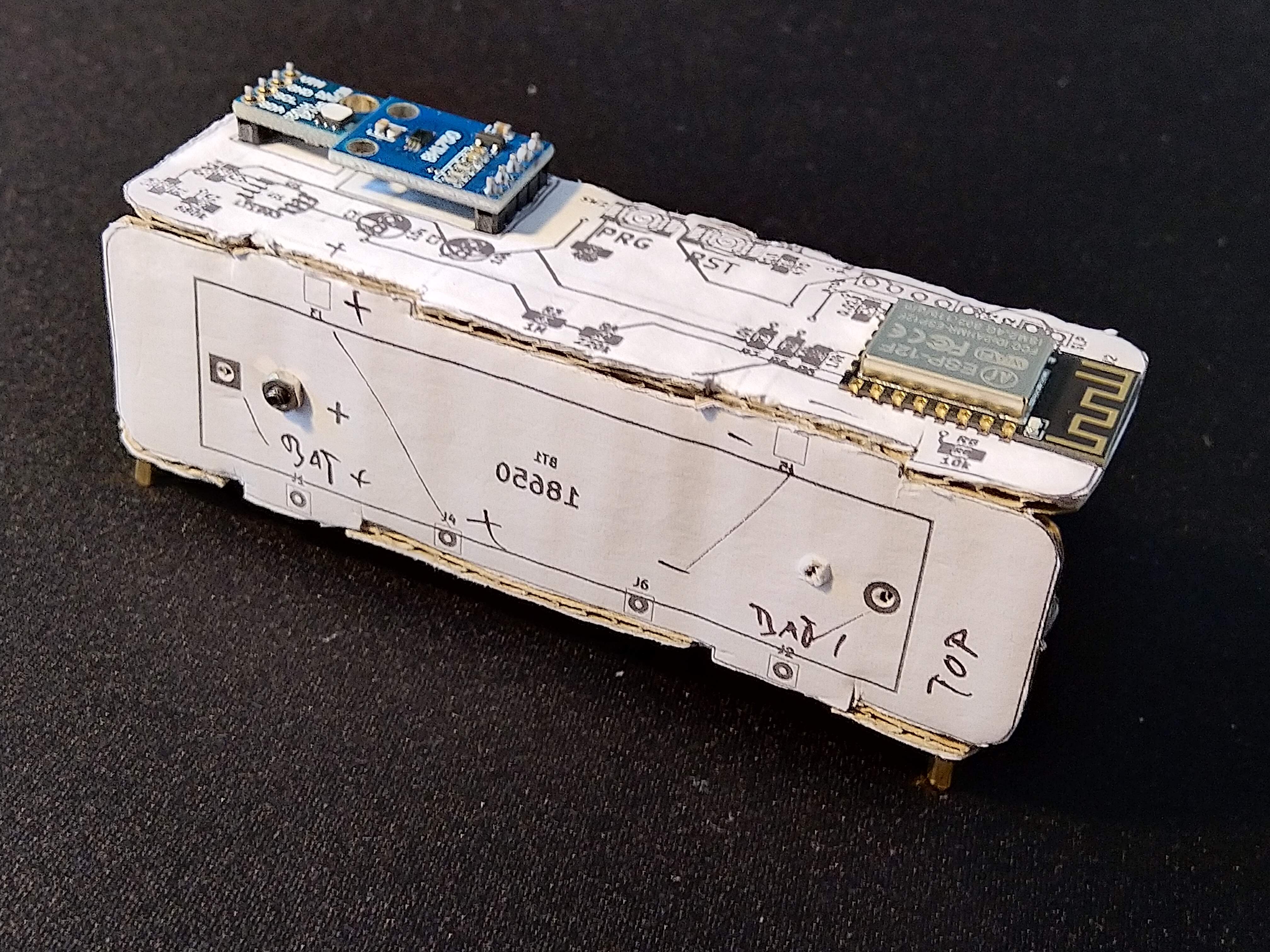
In order to make sure I place everything on properly side and used correct footprints, I printed all the boards and created a cardboard prototype.
After triple checking everything, I finally ordered prototypes. It would be possible to join all three boards into one design using mouse-bites but since the prices for prototypes up to 100 x 100 mm are crazy low, I have just ordered PCBs as 3 designs. It took 2 or three weeks and they arrived.

Construction
I am not going to list a detailed bill of materials here. All can be extracted from the KiCad project.
In general, the following is needed:
- SHT21 breakout and BH1750 breakout
- ESP-12F module
- TP4056 charging and protection module for 18650 Make sure you buy the one with the protection chip, some models have only the charging part and not the protection. You should never connect a Li-On cell without protection a circuit.
- bunch of 1206 resistors (see the schematic for values)
- a few 1206 capacitors (see the schematic for values)
- 2 THT electrolytic capacitors (10uF)
- few pin headers (female) or you could solder the sensor boards directly to the board
- a switch and 2 buttons
- cell holder for 18650
- a Li-On cell (18650)
Firmware and infrastructure.
The firmware is basically the same as described in the previous article.
The device measures the values from sensors and sends them using MQTT to another device (a Raspberry Pi) in my home which propagates them to io.adafruit.com. The client device is on my desk and I recently updated its firmware so I can switch the information I want to display (currently it can display only temperature, but it is possible to switch between rooms).
Future ideas
Right now I don’t have any further plans for this project. But it is possible I might build a freeform variant in the future and there is always something to improve in the firmware.
This article is Part 3 in a 3-Part Series.
- Part 1 -Freeform ESP8266 OLED MQTT client
- Part 2 -ESP8266 based room-conditions monitor, Part 1
- Part 3 -ESP8266 based room-conditions monitor, part 2: PCB