I designed my first PCB. It’s not useful at all and very primitive electrically. But I have learned a lot.
Starting with PCBs
All my projects are on a breadboard and some of them are later transferred to a prototyping board (perfboard). Recently I realized I might give them some more interesting and fancy look in the form of a free-form sculpture or whatever you want to call those. I had no experience with PCBs and I had considered them to be a bit overkill for my projects.
As I was ordering a fabrication of PCBs for my Corne Keyboard I realized how cheap manufacturing of a small set of boards is nowadays. I was also working on a third prototype for my room-conditions-monitor project (no blog post for this one yet, but there will be one soon) around that time and spent a few hours connecting components on a perfboard. I realized it would make much more sense to quickly design a simple PCB and order it from China. The shipping time is not that bad - around 2 weeks for me. That might be a a problem for someone but given the low amount of time I can invest into my projects and also the fact that I often order components on Aliexpress and I have to wait for those, the longer shipping times are not so big problem for me.
So I decided to learn how to make PCBs. My experience with KiCad was: open a project made by someone else, play with layer visibility and pretend I am trying to understand what’s going on, give up, export Gerber files and order PCBs and hope everything is correct. Therefore, I wanted something simple. Maybe I could make a simple funny shaped PCB badge with a coin cell and some LEDs. Nothing original, but originality is overrated.
Squid
Since my girlfriend likes to draw and paint and she is a big octopus and squid fan, I asked her to draw a few sketches for me. The results are super cute.
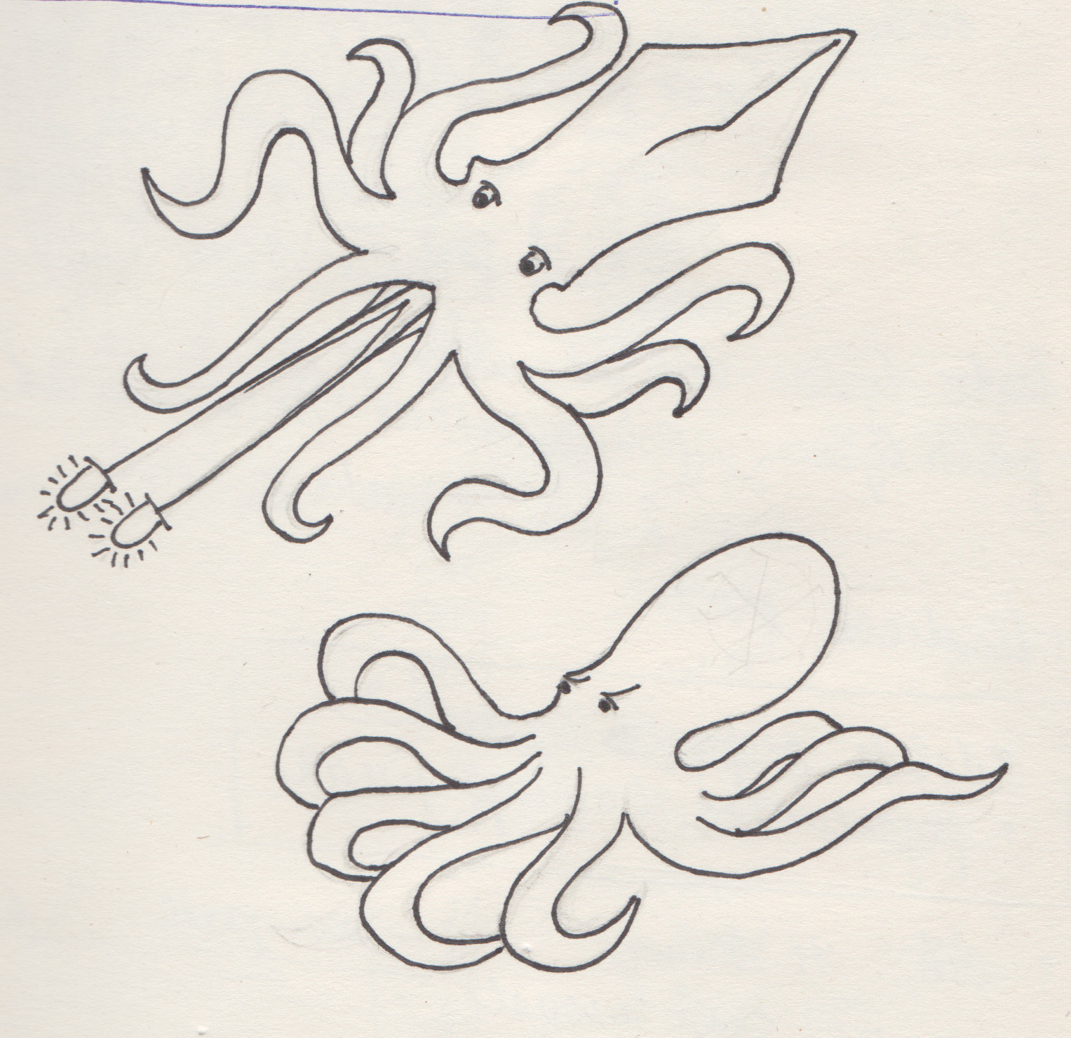
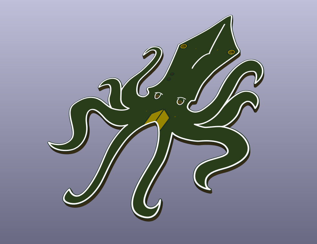
The first step for me was to scan the image into a computer and recreate it in vectors using Inkscape. I already had some experience with Inkscape so that was not a hard task for me. I fixed some details and created several layers with various features (body, silk, other details). The resulting SVG image is available on Github.

The circuit
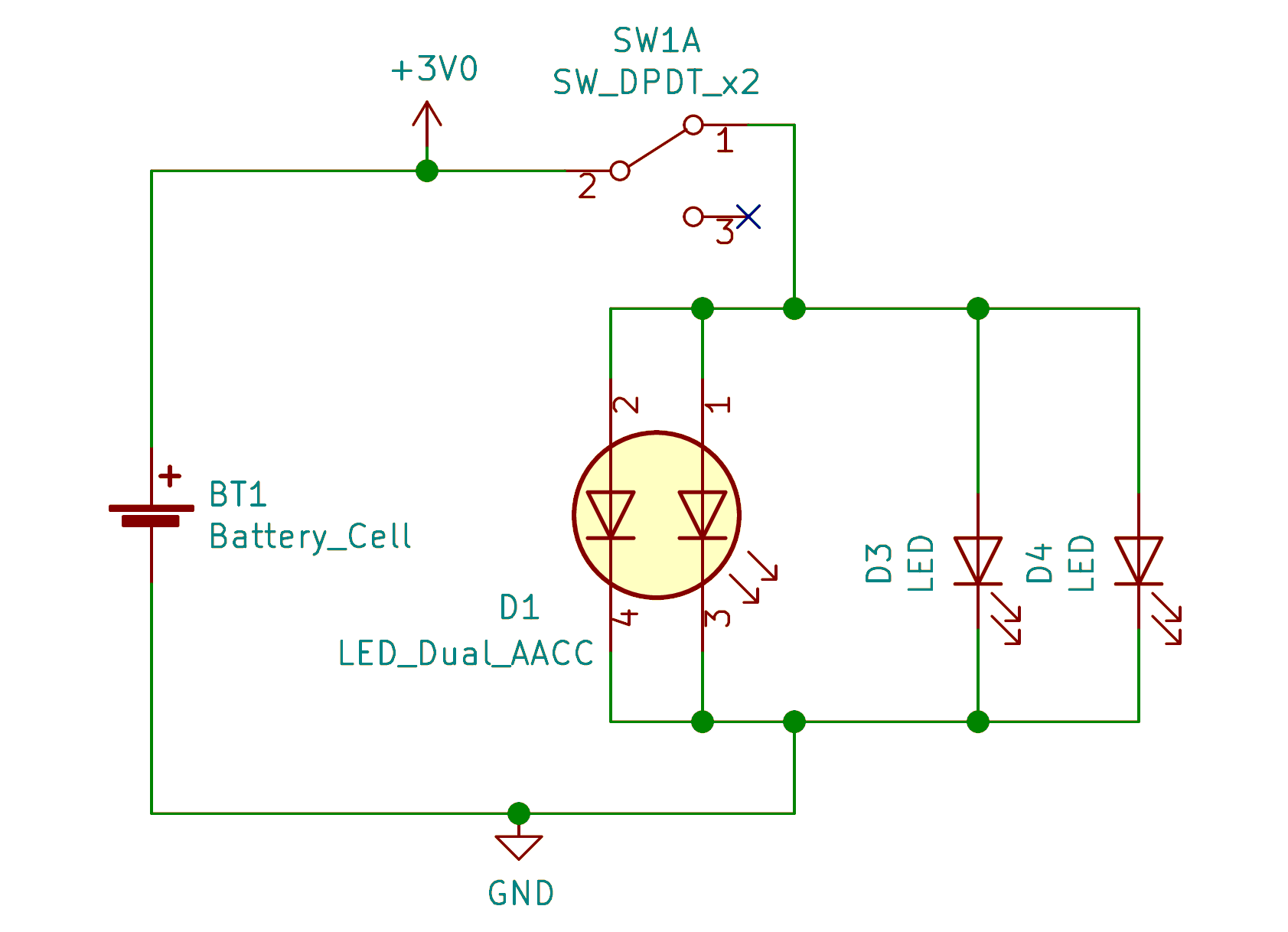
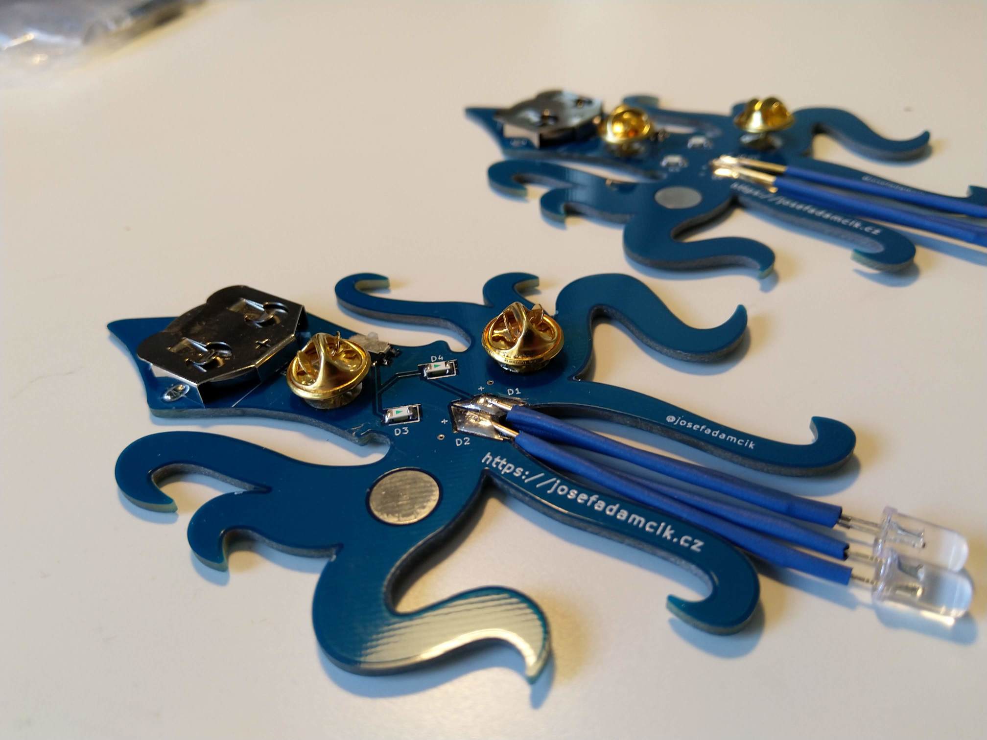
As I mentioned I wanted to go for something super simple. So it’s composed just of:
- a coin cell
- 2 surface-mounted LEDs, those will shine through PCB material in the place of eyes
- 2 THT FLEDs (flashing LEDs, they contain a small chip and flash on they own) for tentacles
- an on-off switch
That’s it. There are no current limiting resistors for LEDs since they are not really needed (A coin cell battery has some internal resistance and will not provide enough current to destroy LEDs.).
Designing the PCB in KiCad
I took me some time to figure out how to transfer the sketch to KiCad. I had to learn general basics of PCB design (PCB design tutorial by Davil L. Jones (EEVBlog) helped a lot), learn some basic KiCad usage and also figure out how to make an unusually shaped PCB.
Those three articles helped me a lot to find a way to go:
- A Practical Guide to Designing PCB Art by Uri Shaked
- Creating Custom Footprints For KiCad by Gabe
- The Turbo Badge PCB Design Experience in KiCad
Custom footprint
I had to experiment a bit (One of the mistakes I did was that the squid was too small for a CR2032 coin-cell holder and I had to enlarge the source SVG and redo everything again. A lesson from this mistake is that I should have printed the SVG and tried if all the components fit before investing more time into the design process.) but in the end, I decided to create a custom footprint for almost the whole octopus.
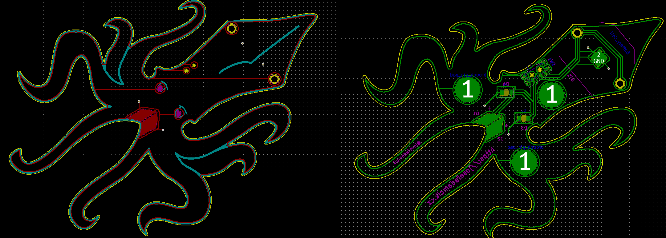
For those not familiar with KiCad or PCB design - a footprint represents a component which is going to be soldered on the board. It has several layers in the same way as a PCB which describe where will be copper (pads), solder mask, silkscreen, and holes. When you design a PCB you start by assigning footprints from database to every component in the schema. Finally, you layout those components on the board and connect them with traces.
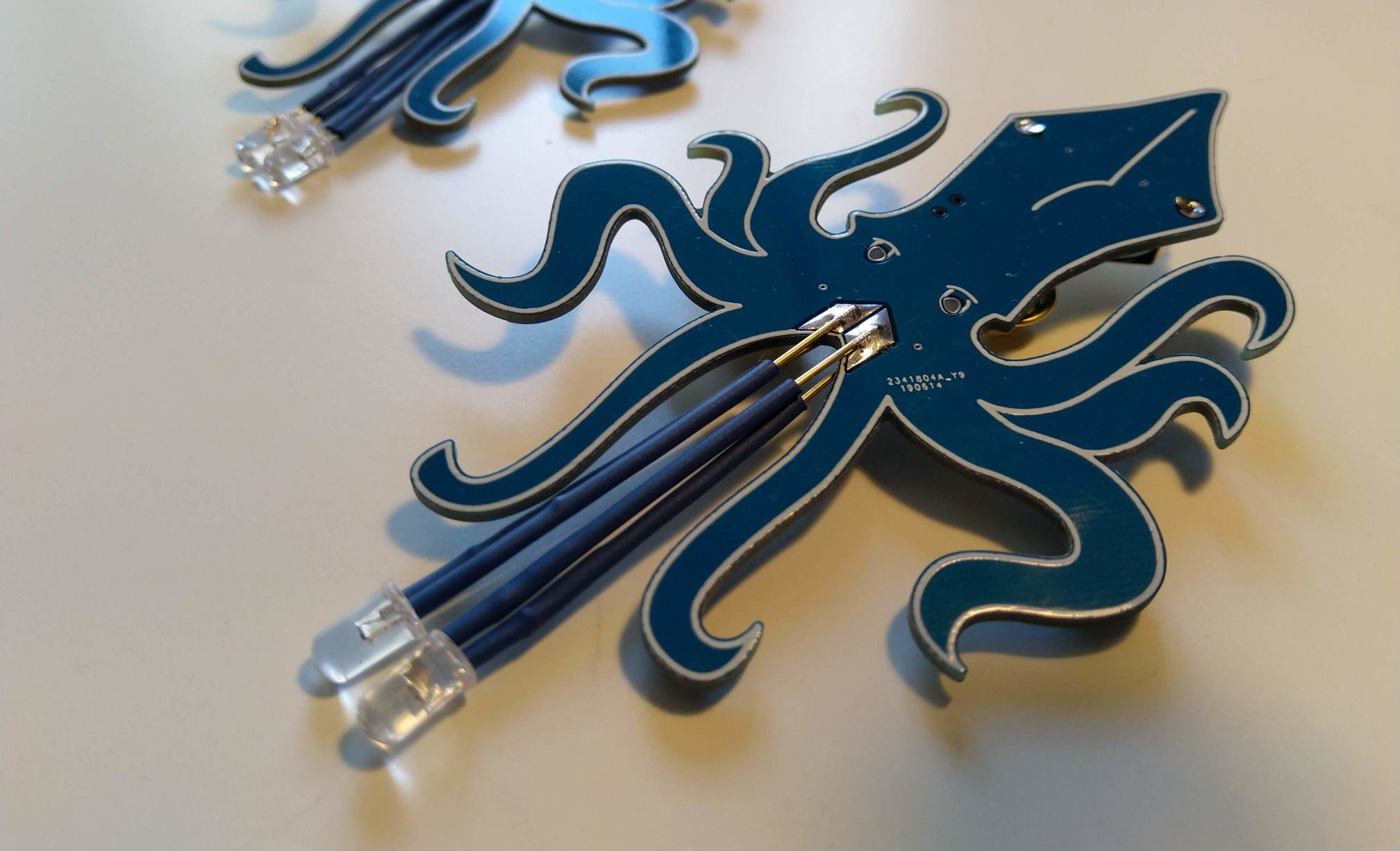
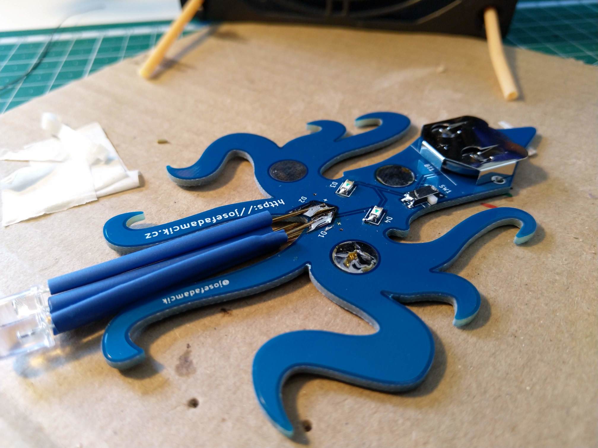
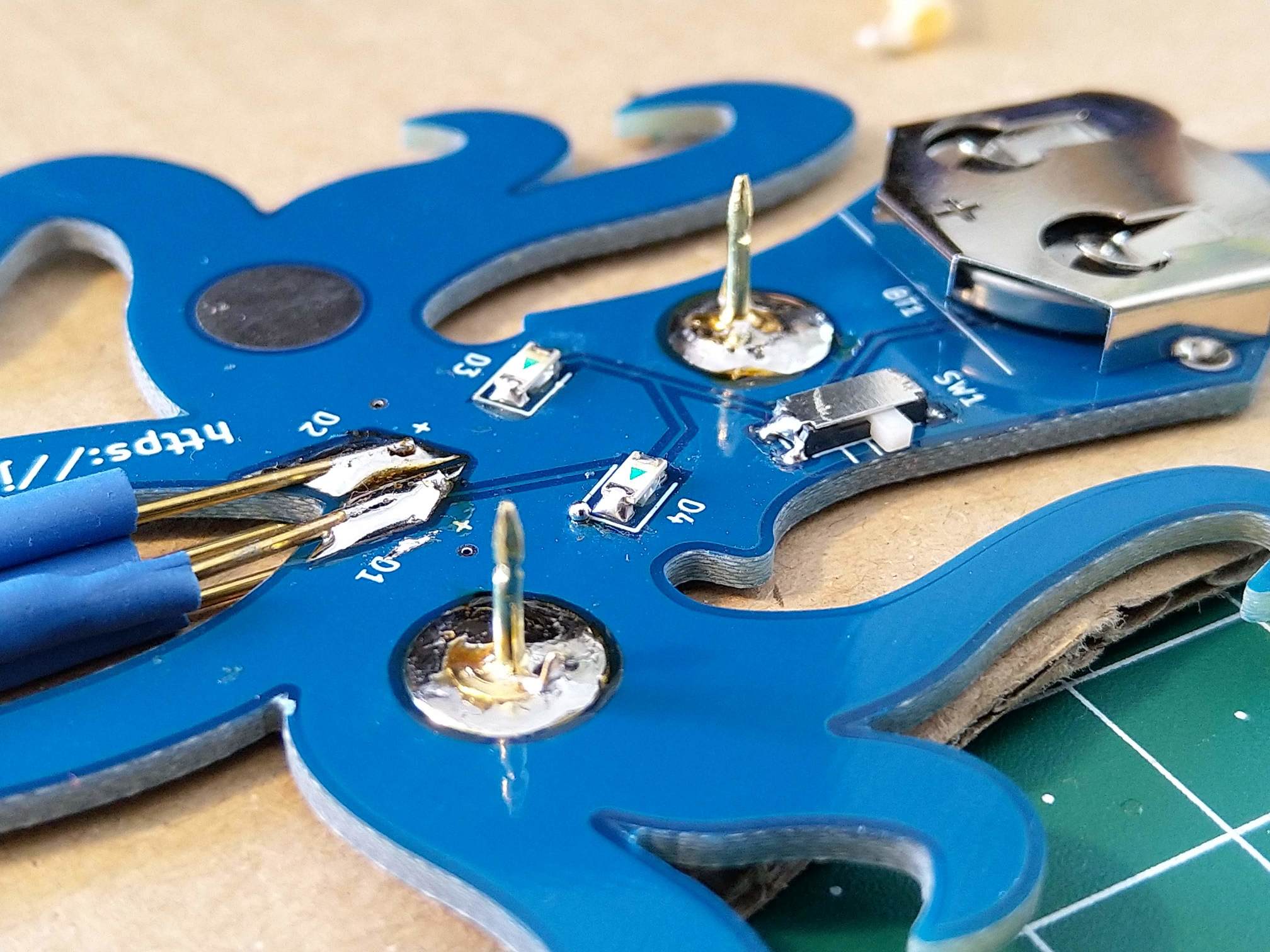
I utilized an Inkscape plugin svg2shenzhen to create a custom footprint for the squid which contains silkscreen for squid’s contour and details, copper pads for tentacles (FLEDs), and eyes. Eyes are special because I wanted to have a bare PCB material visible from both sides so the light from SMD LEDs on the bottom would shine through. That means we need to make sure there’s no copper and no solder mask. Because the footprint contains pads where the 2 FLED tentacles are going to be soldered on (positive on the bottom and negative on the top) I had to use a double-LED symbol (D1) in the schema so that I could assign my custom squid footprint to the symbol and connect the pads as usual.
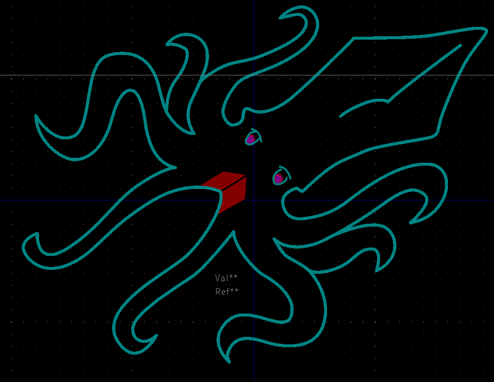
Apart from the Squid footprint, I also created a footprint for SMD LEDs with a hole for the eye for the bottom side and a footprint for a rounded pad which will allow me to solder a brooch pin (Aliexpress) on.
Putting it all together
I have also exported a shape for the Edge.Cuts layer (contains the overall shape of the board) and imported it into my project. This can be done either by using svg2shenzhen Inkscape plugin or just using basic Inkscape capability to export into a DXF file as described A Practical Guide to Designing PCB Art by Uri Shaked (look for “Creating The Base” section).
The whole KiCad project including libraries with custom footprints is available in a Github repository. I am not going to go through the whole process here but I’ll share a few remarks.
- The copper pour for ground zone: both sides have unused areas filled with copper acting as ground. This is done by selecting a zone which should be filled in and the rest is calculated by KiCad. In my case, it was a bit more complicated, because I needed to keep squid’s eyes copper-free on both sides. I have solved this differently for every side. The top one has (as a part of the squid footprint) small copper rings around eyes. When KiCad fills the zone it avoids any copper from footprints with some clearance. On the bottom side, a more straightforward approach is used - I just defined two keep out areas which forbid the auto-fill around eyes.
- I made a mistake when placing the coin-cell holder. It’s rotated to fit the head of the octopus nicely, but if it was soldered properly the opening for a battery to slide in would be at the left-bottom side. There would be other things soldered on (switch, pins) and it wouldn’t be possible to insert the battery. I didn’t realize this until I had manufactured PCBs in my hands. But the fix is easy - the battery holder just needs to be rotated 180 degrees so the battery could be inserted from the top-right side.
- You may notice that the round pads for brooch pins are not connected to the ground plane. I left them disconnected to make soldering a bit easier (heat cannot escape to the GND plane).
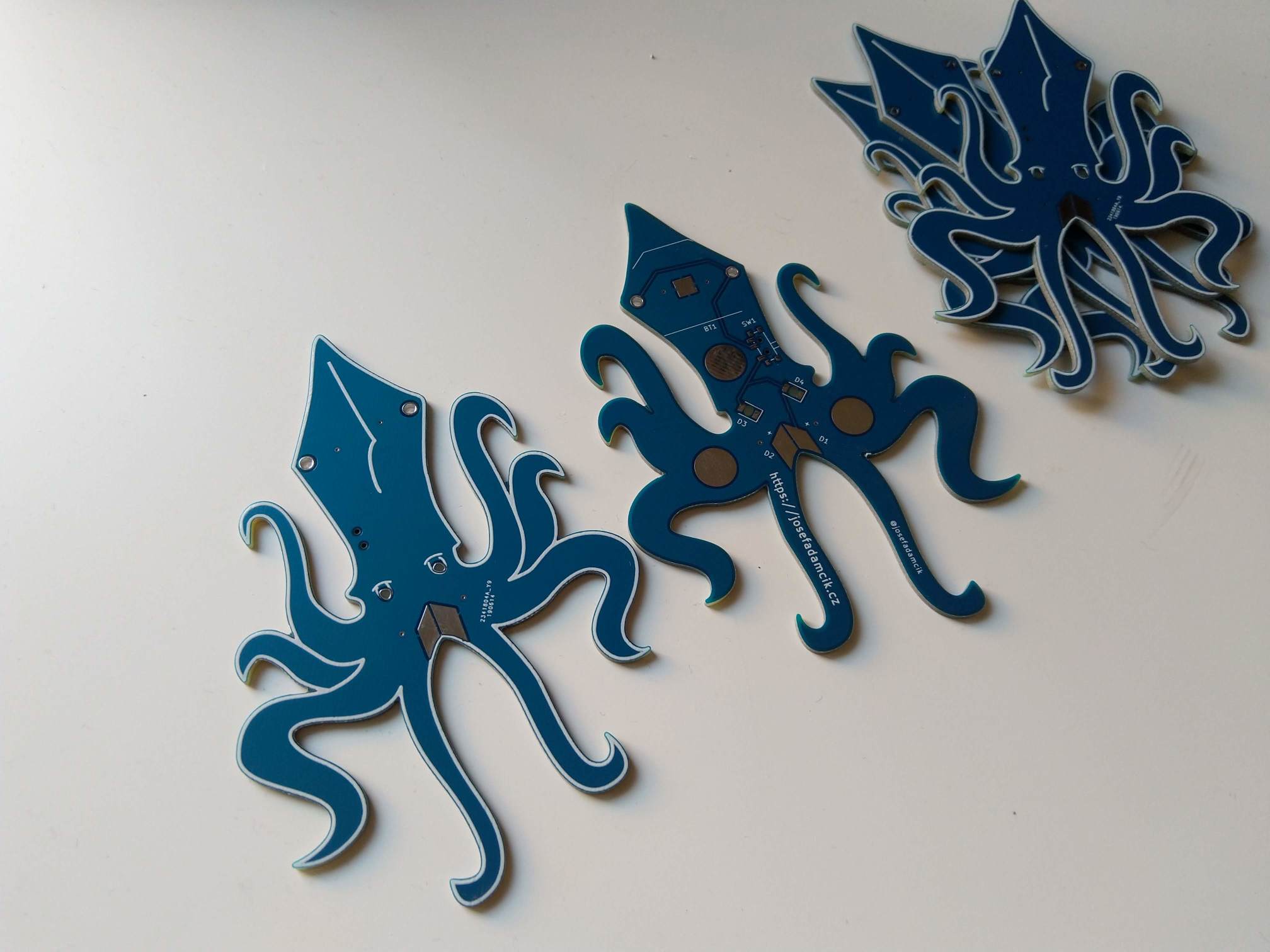
Manufacturing and final boards
The next steps are straightforward:
- double-check everything
- export Gerber files and zip them
- upload the Gerber files to the service (JLCPCB in my case)
- check everything in their web-based Gerber viewer app
- select color in the order form (I left default values for the rest of the fields.)
- finish the order and wait
I was careful to keep the board size under 10x10 cm to have the cheapest price. I ordered 5 (the minimal amount) of boards for 1.78€ (2$) plus basic shipping (5.19€ to Germany). Crazy cheap.
And time-wise?
- 14.6. - placed the order
- 15.6. - boards were manufactured
- 16.6. - they were packed and waiting for pick-up
- 18.6. - delivery started
- 27.6. - delivered
That makes 13 days from placing the order to delivery. That’s fast enough for me.
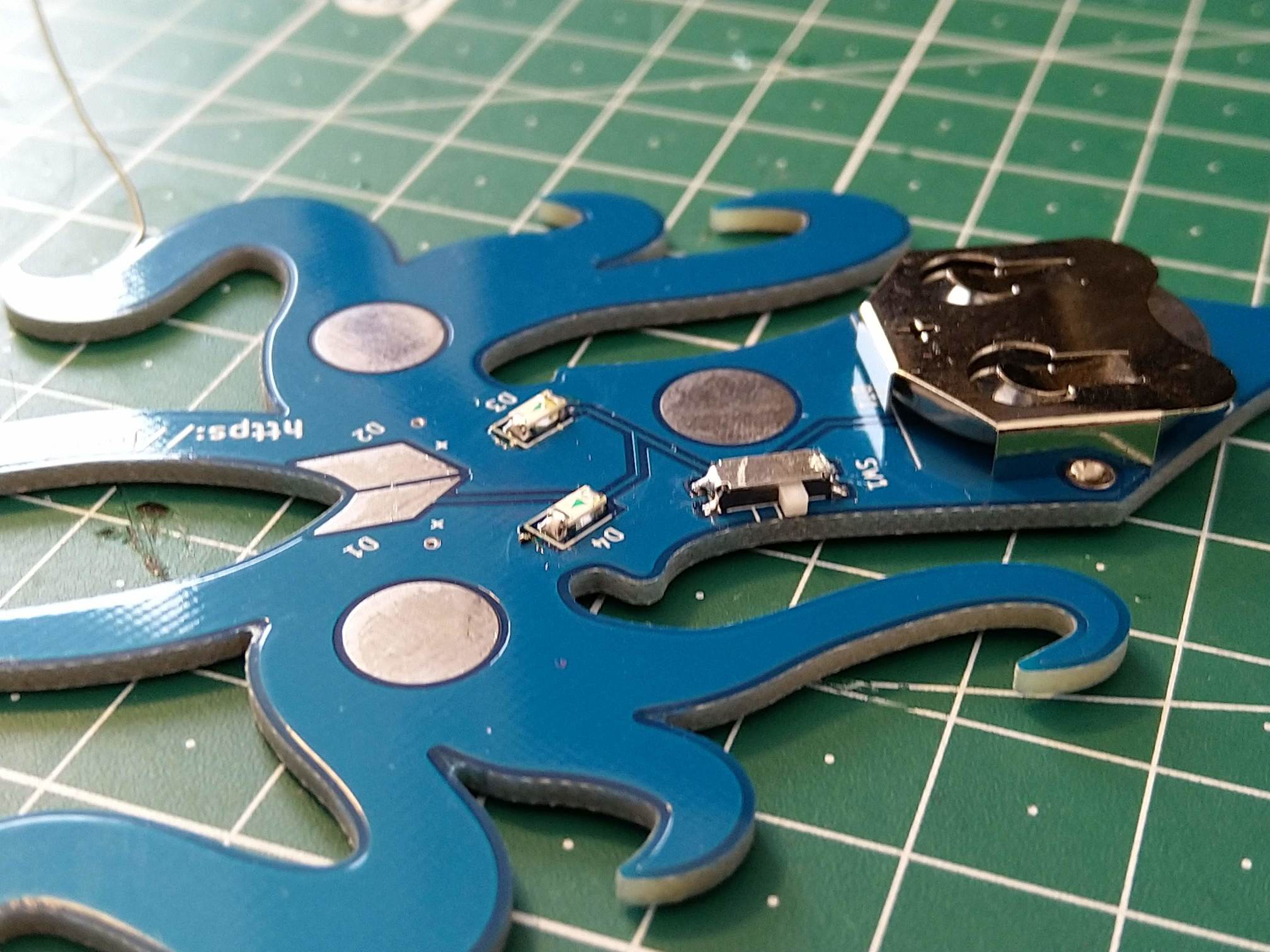
Building the Squid
Bill of materials
For each squid, the following is needed (the links below are just for the components I ordered and used, they are not affiliate links):
- a PCB Github repository with the whole KiCad project
- CR2032/2020 THT cell holder (Aliexpress)
- SMD switch (Aliexpress)
- 2x THT FLED (Aliexpress)
- 2x SMD LED 1206 (Aliexpress)
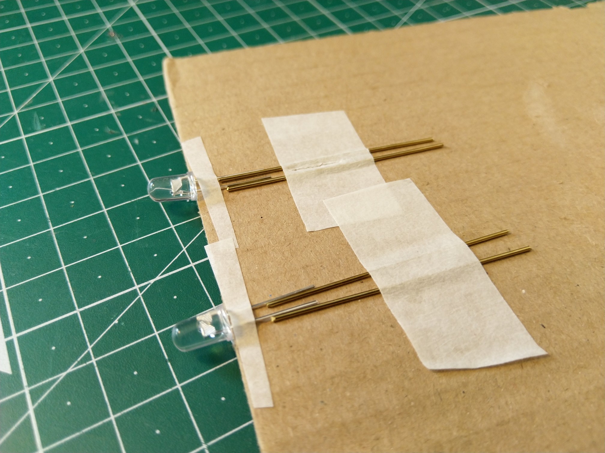
- 4x piece of 0.8mm brass rod, length 4cm or some stiffer wire
- 4x piece of heat-shrink
- 1-3x Brooch pin (Aliexpress)
- CR2032 coin cell
Build log
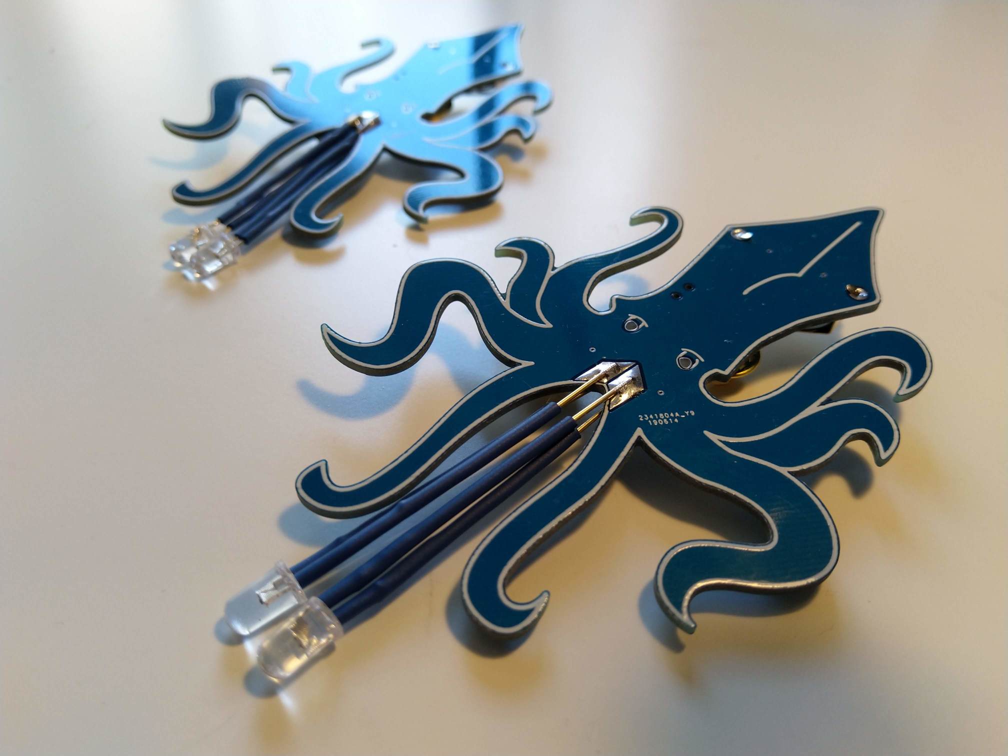
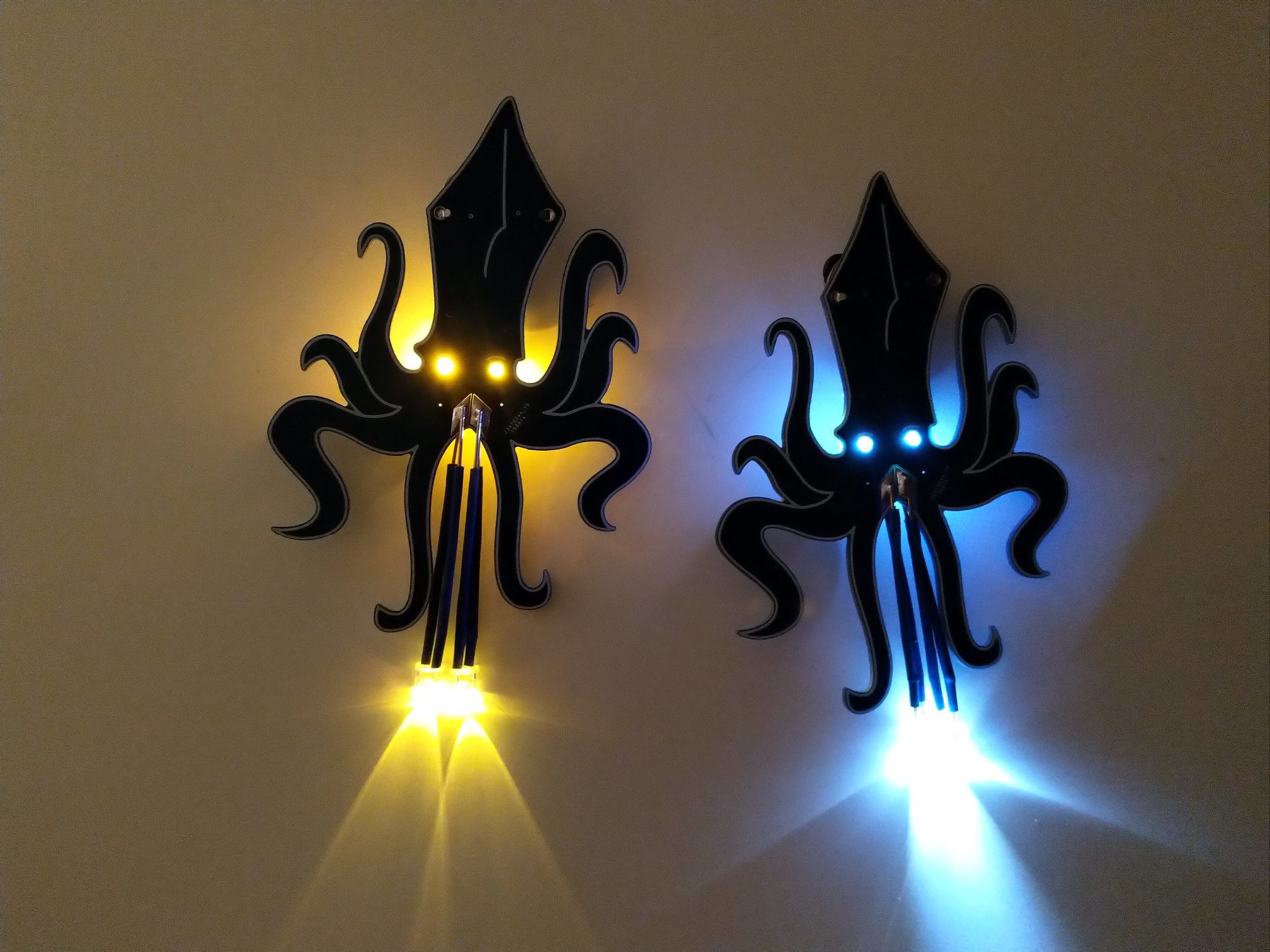
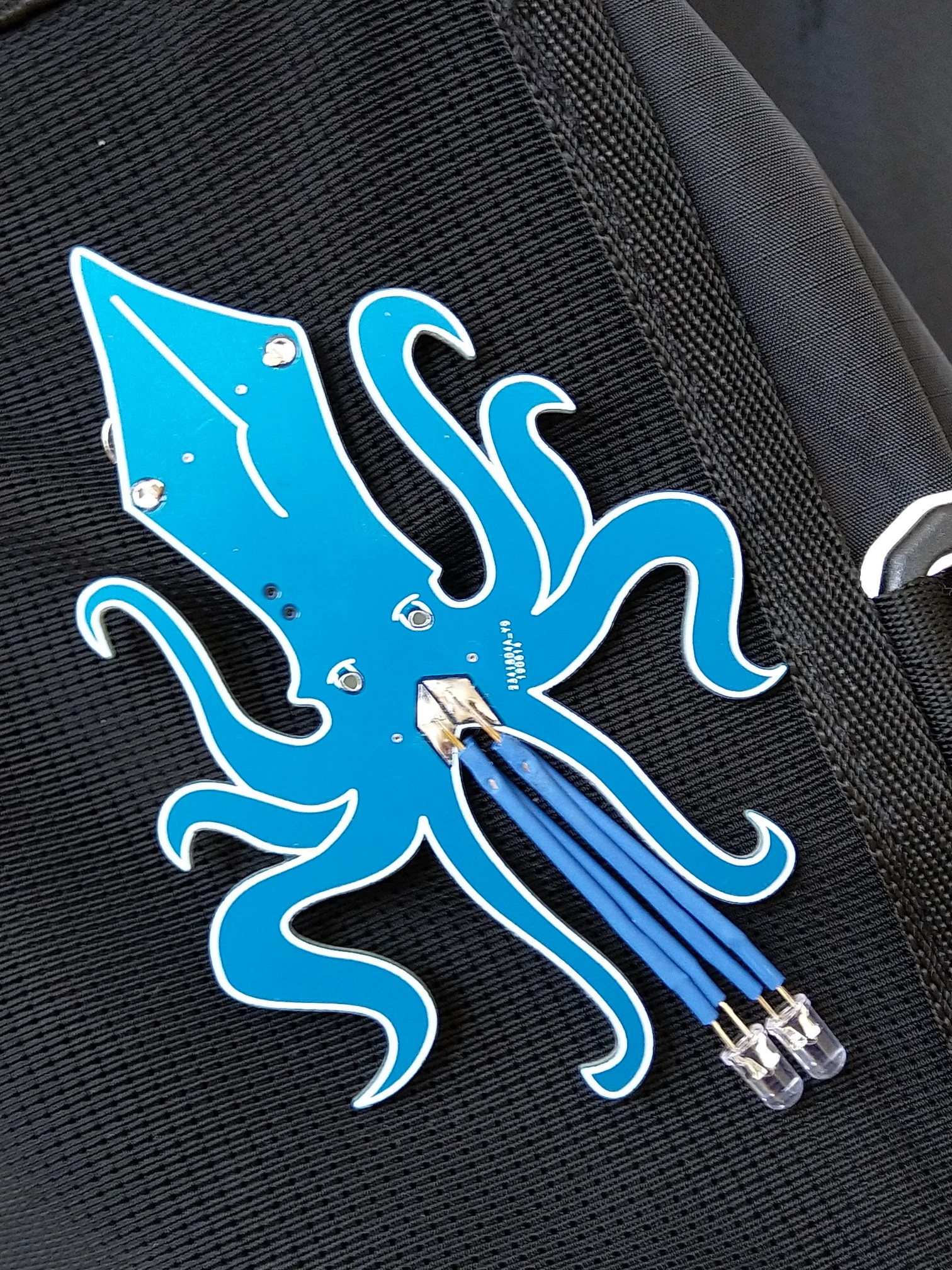
The final result
Next plans
There might be a second revision of this badge which would solve some issues and improve the design a bit.
But more importantly, I really enjoyed designing and building this small silly thing and I really want to make more designs soon - more complicated and more interesting ones. My girlfriend seems also interested and she is already sketching some new ideas. I am really looking forward to the next one.
If you are interested in our next creation too, you can always follow me on Twitter or use an old-school RSS feed and subscribe to updates on this blog.