I have enjoyed designing and making a Squid PCB badge some time ago and I have some plans for more complex PCB badges and creations. But Christmas is coming and I realized it might be fun to create some simple gift for friends and family. It was also a good opportunity to try another PCB manufacturer.
PCB design
Schematic and functionality
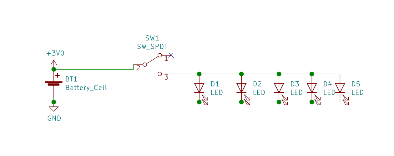
The schematic is similar to the Squid badge. No logic, no microcontroller. Just a few LEDs, a coin-cell and a switch.
There are no current limiting resistors which is theoretically incorrect. But I went with such simplification because based on my experience (and now only mine: check out jewellery by Jiri Praus for example) it’s not an issue. It’s mainly because:
- White LEDs drop around 3V which is the same as voltage of the battery. Value for the resistor would be theoretically 0 (but I could use some low value).
- I also used yellow LEDs which drop only 2.2V but the coin cell battery wont’ provide enough current to hurt them. Things like internal resistance and other imperfections in the battery intervene. But this is kind of moving on the edge, you can have problems with some better batteries when only one LED is connected. It’s safer to solder all LEDs before connecting.
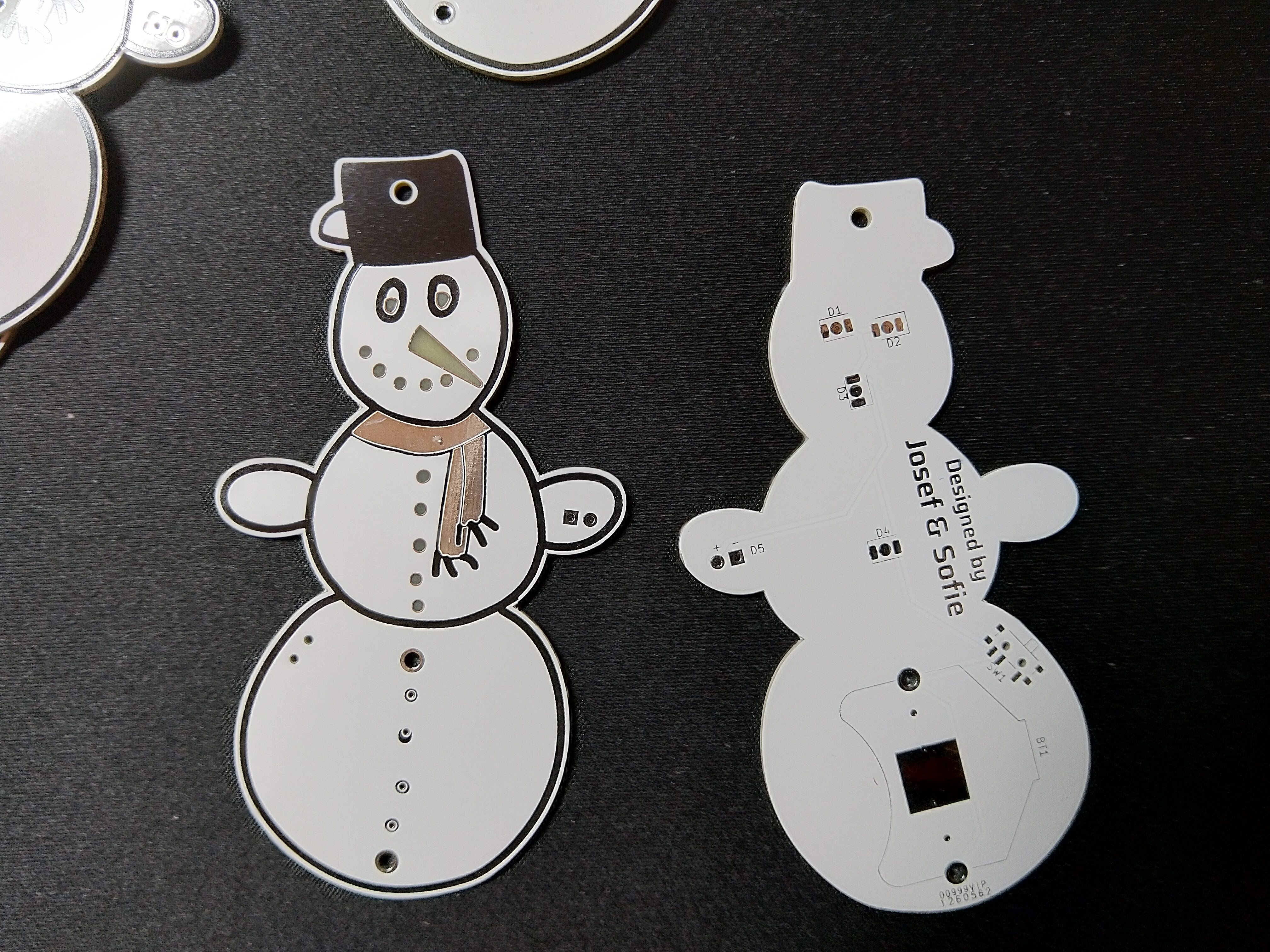
The PCB would use a white solder mask and black silkscreen. I have also incorporated bare copper with HASL finish1 for snowman’s scarf.
Drawing in Illustrator
My girlfriend was so kind and sketched an image of a snowman for me. She even converted it into a vector image in Illustrator. Sadly the export from Illustrator to SVG was not exactly what I needed2 so I still had to do a bit of work in order to convert the source image to a simple set of paths.
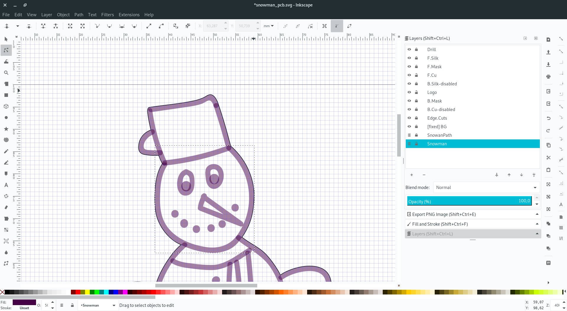
As soon as I had simple paths drawn, I used the Svg2Shenzen Inkscape plugin to help with PCB design in Illustrator. This plugin is very easy to use. In the first step it sets up an empty document - the plugin will create properly named layers for you. Then you draw into layers what you need and finally, you export them to either a KiCad project or a KiCad footprint.
I wanted LEDs to shine through the PCB material in a few places: eyes, nose, mouth, and buttons on the snowman’s chest. That required me to ensure there is going to be no solder mask nor copper on either side of the PCB. I included the front copper layer (F.Cu layer in Inkscape, red on the image below) for the head and chest in the SVG with holes in all required places.
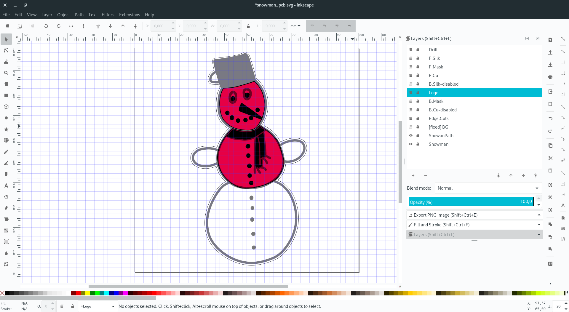
I have also included holes in the solder mask for the front (F.Mask in Inkscape). Keep in mind that in the case of solder-mask we are choosing where we don’t want the solder mask to be (it’s kind of solder-mask mask). So black areas are those without solder-mask.
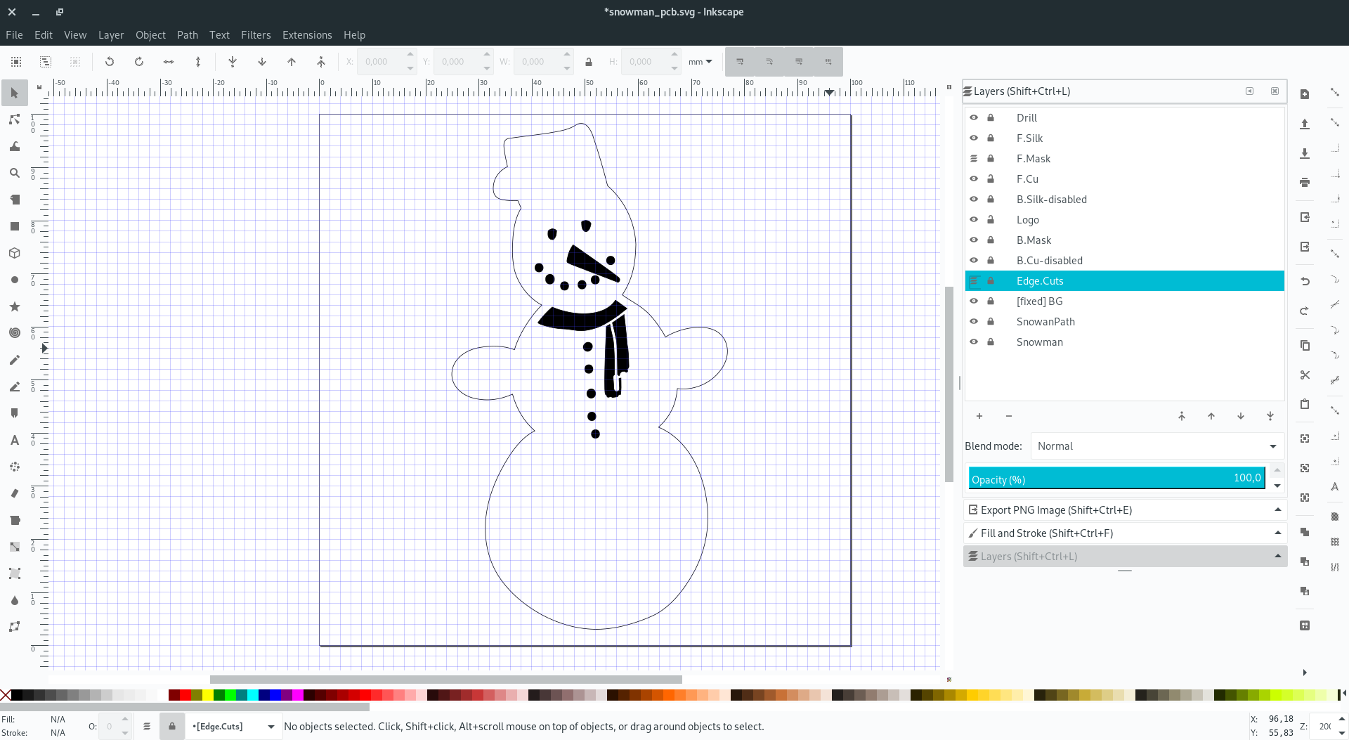
Since the backside should contain all the functional components I didn’t prepare any back layers in Inkscape
The SVG file for Inkscape is available at Github for anyone interested in examining the result.
KiCad
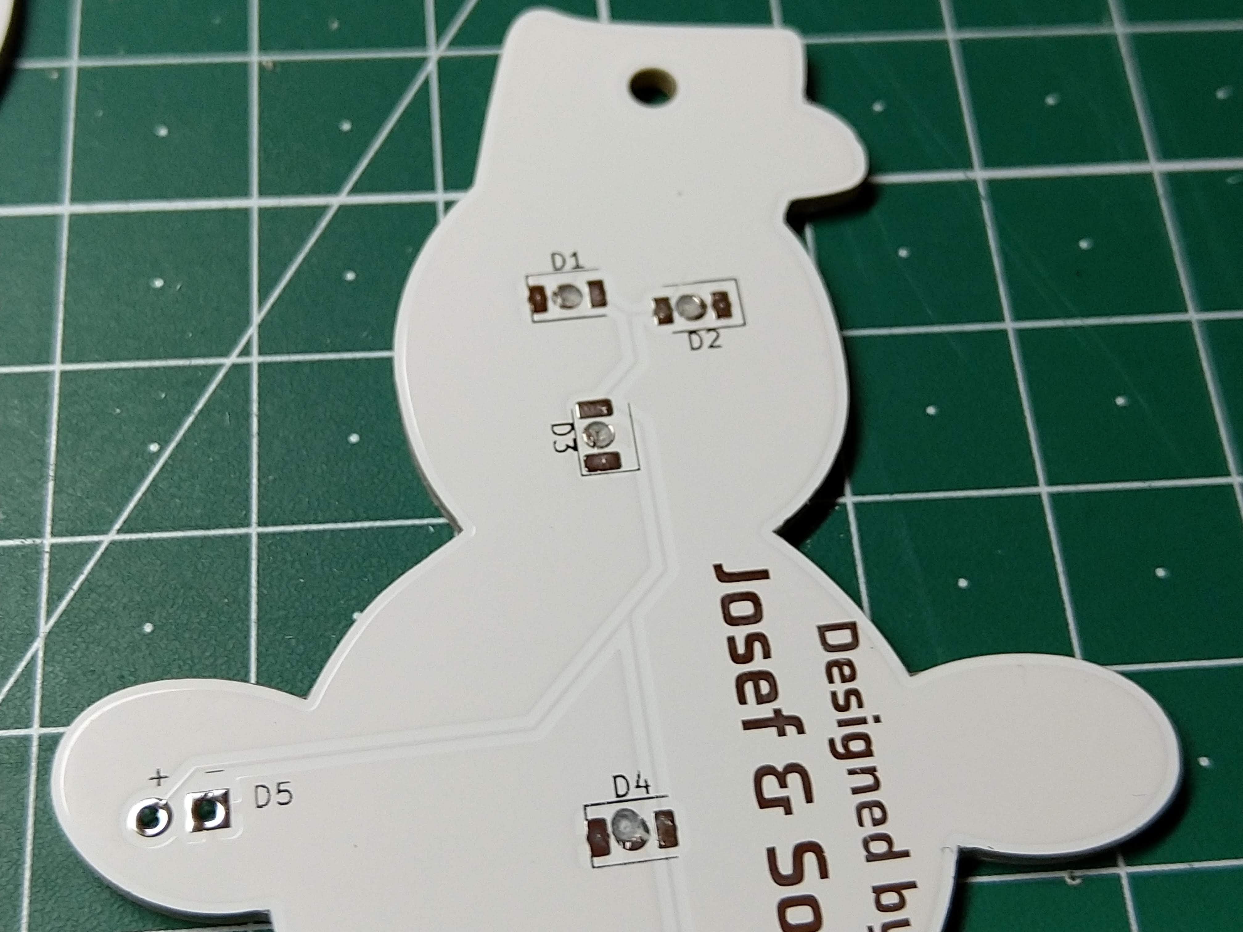
I exported a KiCad project using the Svg2Shenzen plugin and then put together files created by the plugin and my other project which contained the schematic above. I made sure all components have assigned footprints. Once I opened the PCB, I was able to update the PCB from the schematic, place the components on the backside and connect them together using traces. And finally I defined zones for copper pour on both sides.
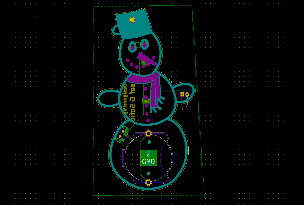
KiCad has a very nice 3D preview feature. It is possible to customize the colors of all materials to have a representative image.

I was very happy with the result so I exported Gerber files and prepared a zip archive for manufacturing. It’s always good to double-check everything so I opened them in a Gerber viewer.
That was a good decision because I quickly noticed that I forgot one important detail. There were no holes in the back copper layer under LEDs so the light would not shine through the PCB as intended.
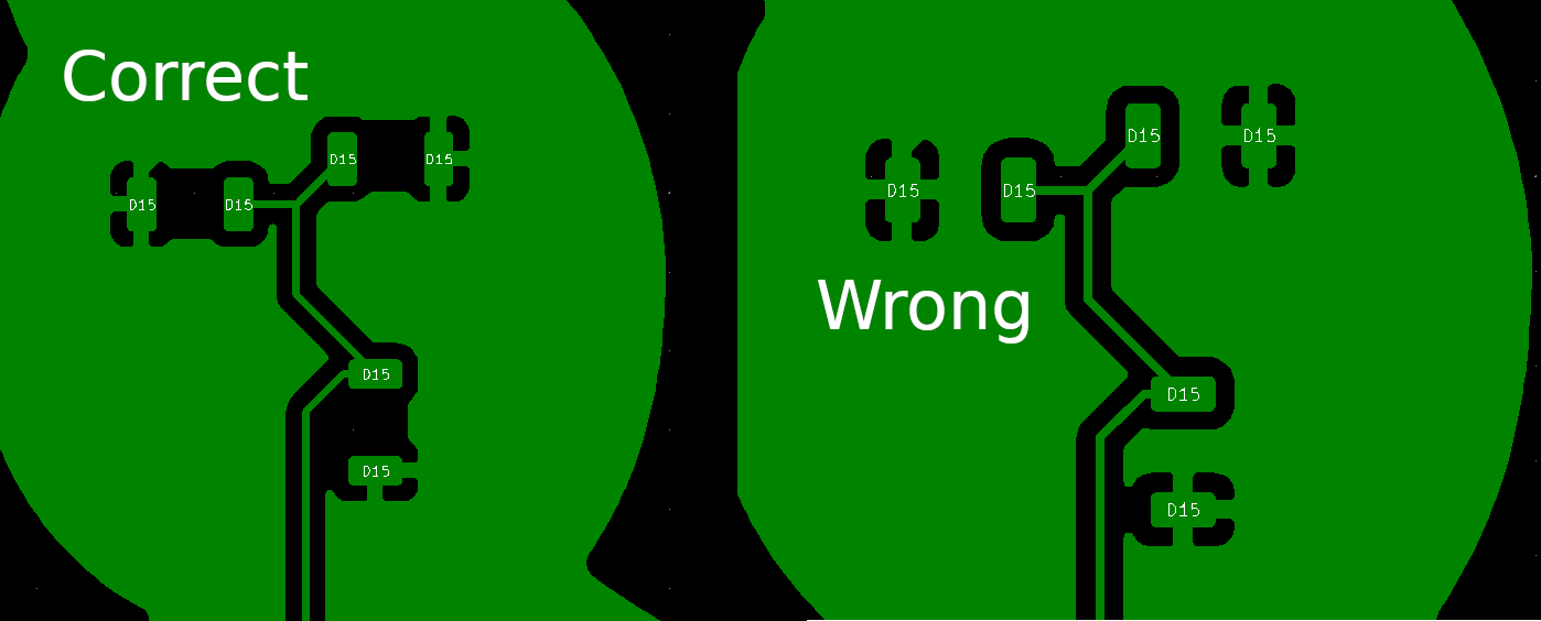
The fix was easy. I just had to define small keep-out areas for copper on the bottom. It’s important to check the “Keep out copper pours” option when setting up.
I didn’t have care about solder-mask since the custom footprint for LED I have used already deals with that.
The whole KiCad project is available on Github under MIT license.
PCB Manufacturing at Seed Studio
Seed Studio reached to me and offered me to sponsor a small PCB project if I try their Fusion PCB service and write about my experience. I was happy to try another PCB manufacturer.
Price and order
A set of 5 or 10 boards with basic parameters (up to 100 x 100 mm, HASL finish with lead, basic PCB material and so on) in any solder-mask color is under 5$ plus shipping which is crazy cheap.
I wanted a lead-free HASL finish and 15 boards. Which raised the price a bit to $33.67 plus $12 for basic shipping to Germany. Still a very nice price for bunch a of boards (roughly 2.40$ per board). Seed studio was kind enough to provide a 30$ coupon for my order.
The order process itself works pretty well: upload Gerber files, pick the parameters in a web form according to requirements and finish the order. I have added a note to my order kindly asking the operators to put their internal order number on the bottom of the PCB3.
How long did it take?
- order placed: 21.10.2019 20:52
- file review start: 22.10.2019 04:00
- start of production: 23.10.2019 23 01:03
- PCB finished: 26.20.2019 20:14
- Order packed & shipped: 29.10.2019 09:13
- Shipment picked up by delivery company 30.10.2019 05:01
- Arrived 11.11.2019
So from order to shipping, it was 9 days that’s not the quickest turn-over I would say. Interesting here is to see, that the PCB was in the “manufacturing” state for 3 days and then it was waiting to be shipped for another 3 days.
I would expect that most of the orders would be still using HASL with lead (because that’s the cheapest option) and if you choose that option you might get much shorter times. For me, it wasn’t an issue at all. It was around 3 weeks including shipping and that matches my expectations and needs.
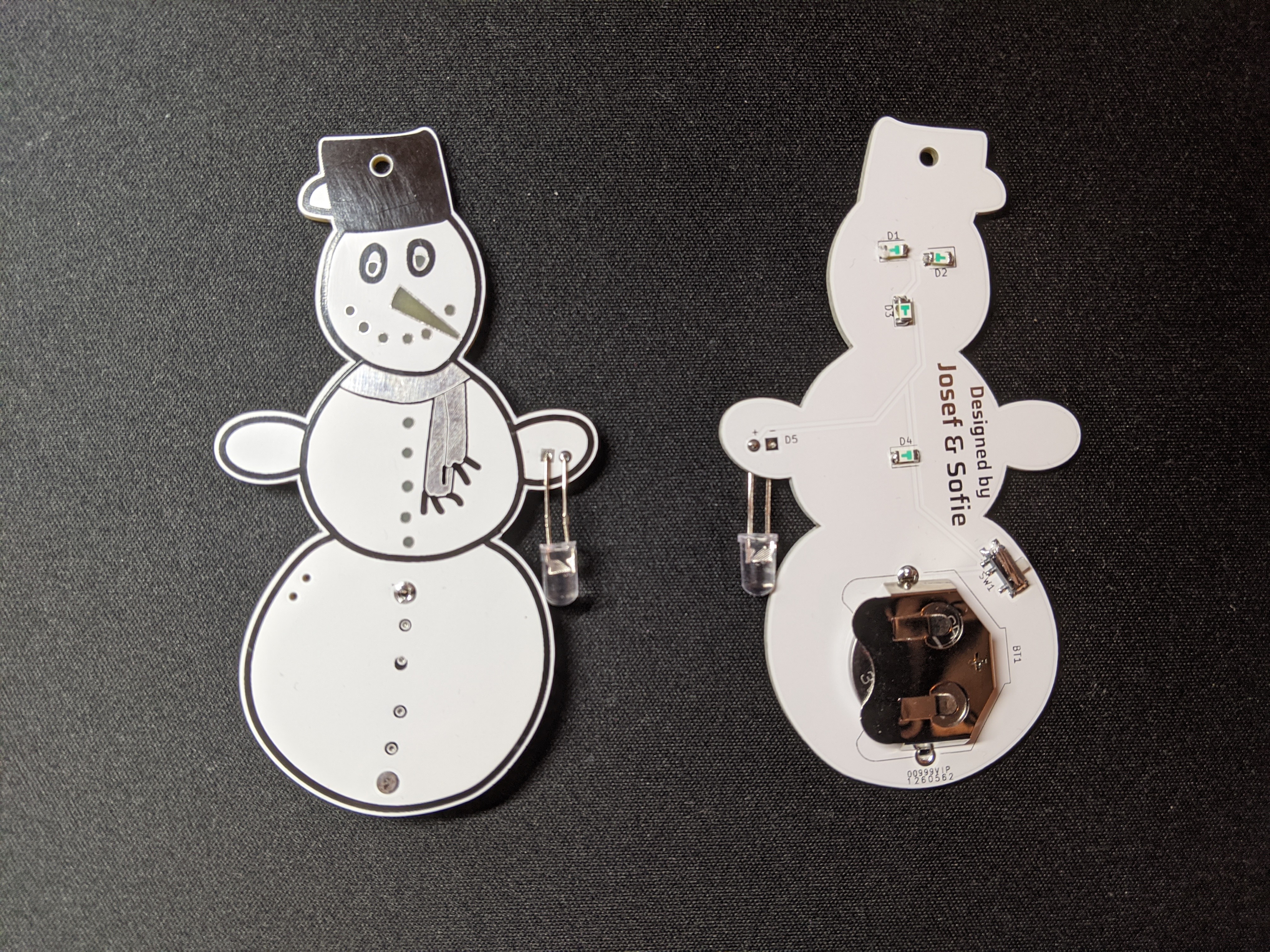
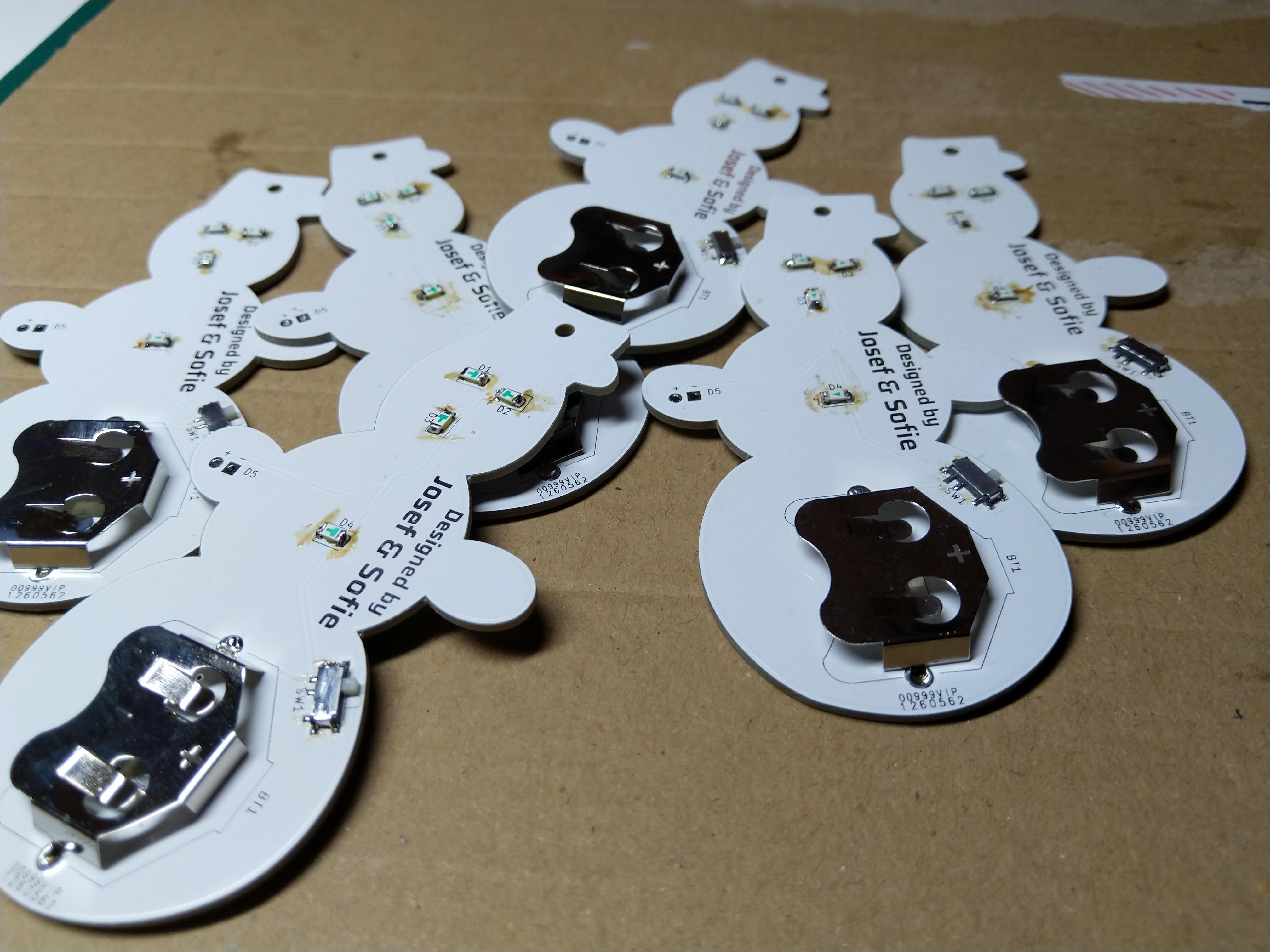
Fabricated PCBs
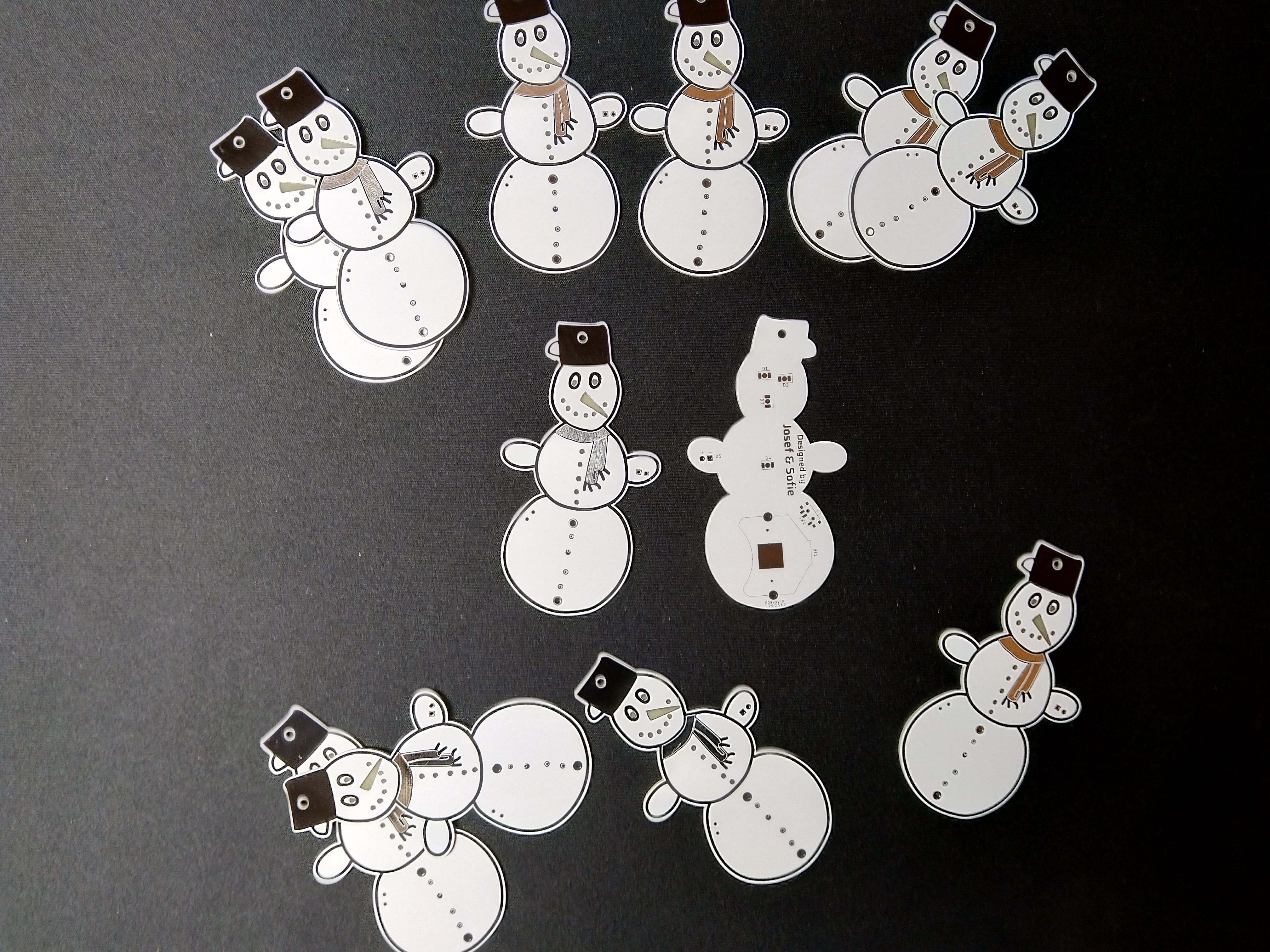
PCBs arrived nicely packed and very well made. I have found no issues and was very happy with the result.
Until I learned that I messed things up. Twice.
Mistakes
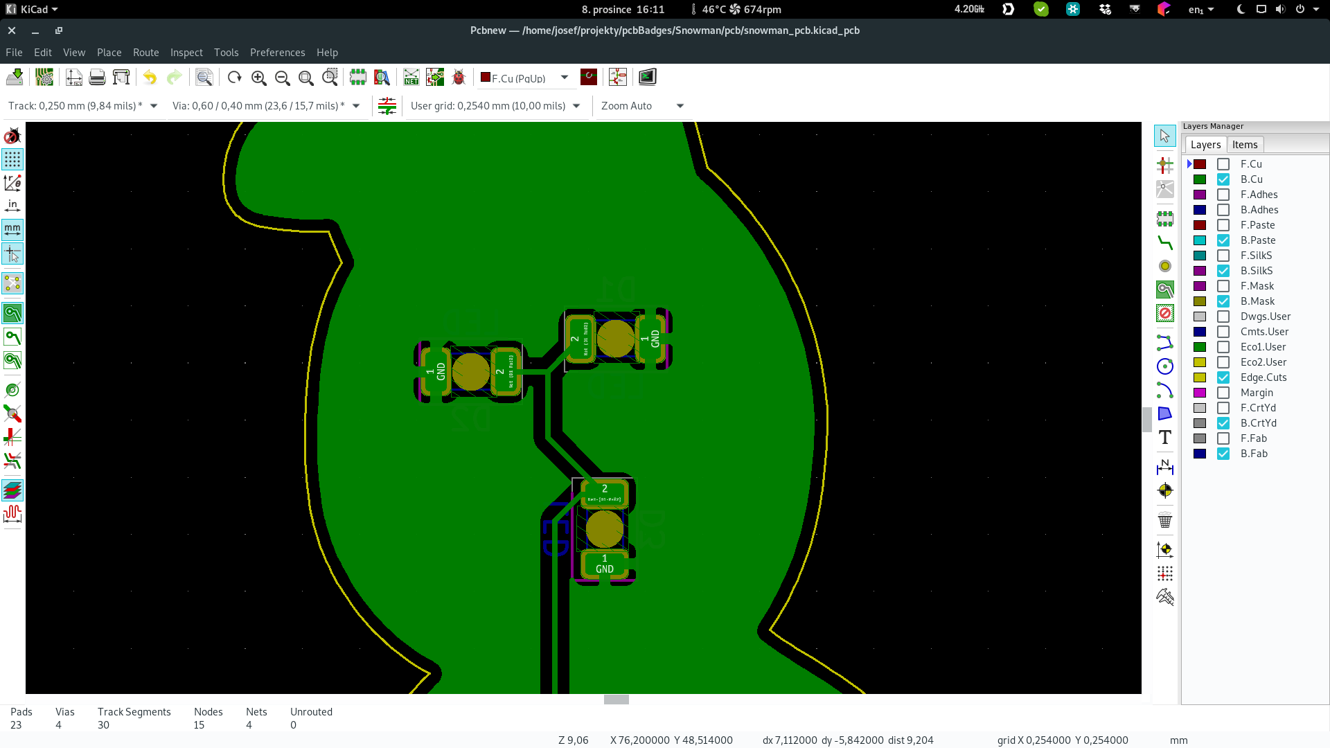
You may notice it on the image above if you look closely at the backside. Do you remember how I fixed the problems with copper pour at the last minute? Apparently, I still messed up during the order and uploaded the old Gerber files. So I have got them manufactured with the error I thought I fixed. Well, I felt like an idiot and was quite unhappy with myself.
Annoying mistake, yes, but not a reason to throw the boards away. I experimented with a few ways how to scrape the copper off and ended up using a drill with a small drill bit and carefully drilled off a bit of copper from each place.
Another mistake was also quite embarrassing. I used the wrong footprint for the coin cell holder. The one I wanted to use was for CR2025 or CR2035 cells which are 20 mm in diameter. But I accidentally used a footprint for a 25 mm cell4.
I could have ordered the right coin cell holders. But I was hoping the ones I already had in my stock and also didn’t want to wait. So I just stretched them to be a bit wider. The price for that is that I can no longer use thicker cells (CR2035) but only the thinner ones (CR2025).
Construction
Bill of materials
- 4× 1206 LED Any color but use only one color on one PCB5
- 1× Coin cell holder I used THT coin cell holders for 20 mm cells from Aliexpress. But the correct one for the footprint would be Keystone 3009 for CR2450
- 1× surface mount slide switch PCM12SMTR (Alixepress)
- 1× THT Flash LED 5 mm Candle yellow (AliExpress)
Soldering
I started with SMD components. LEDs are quite tricky since they have to be soldered the other way around in order to shine through the PCB. I do it by making a big blob of solder on one pad and placing the LED using tweezers to connect to the (molten) blob. Soldering the second pad is much easier since the LED is fixed in place. If needed, I can resolder the first connection as the last step.
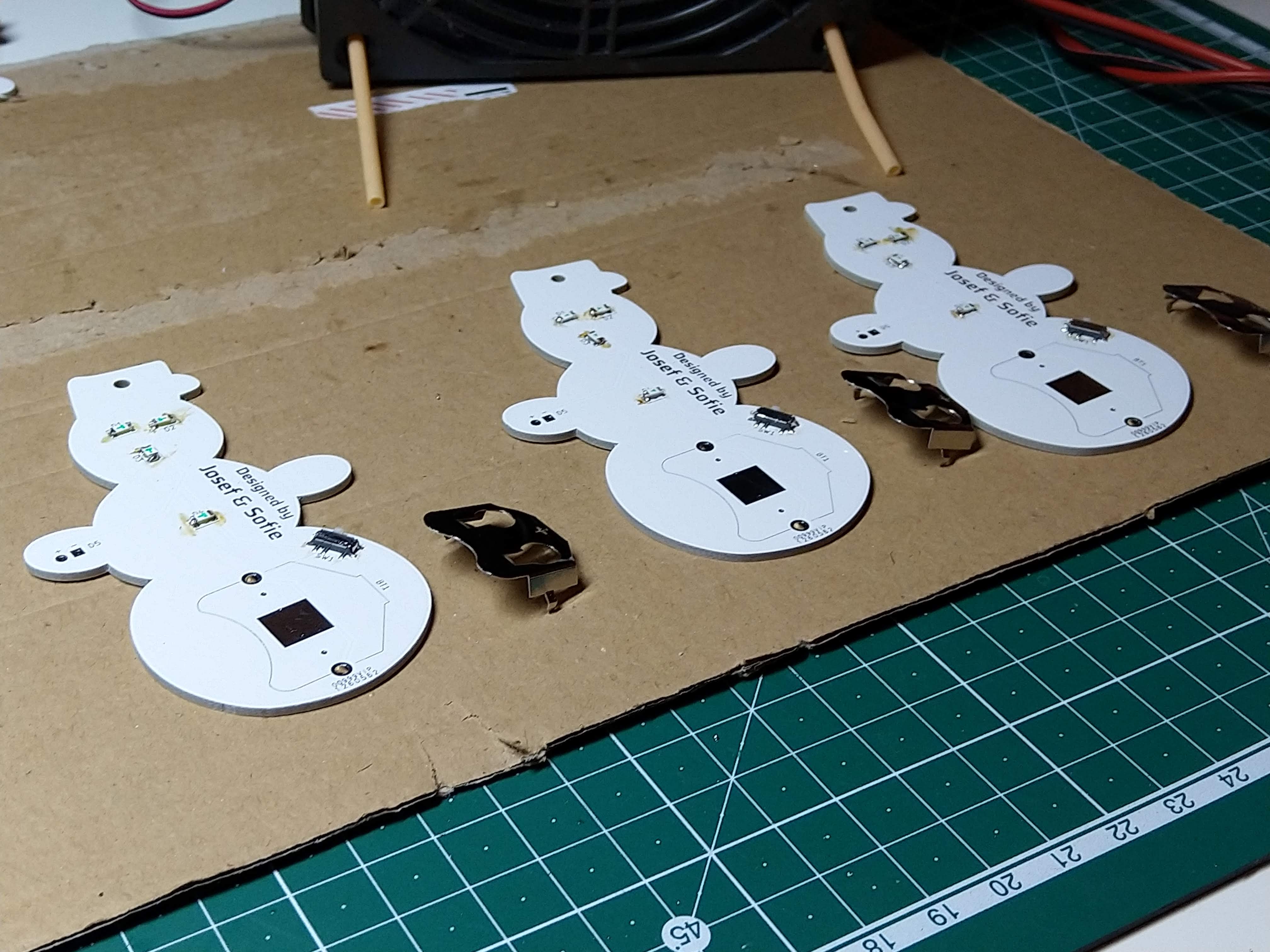
There’s nothing special about soldering the coin-cell holder. For the THT LED I bent legs at their ends to create a small lamp hanging from snowman’s hand.
See them shine
I am quite pleased with the result. Mistakes were made, lessons learned. But overall I like them and I look forward to gifting them.
If you like them, you can make your own. Just open the project in KiCad and roll.
Notes
Links
-
Lead-free, of course. They are going to be gifts for people. ↩
-
I am sure it is possible to draw and export the shape from Illustrator properly. But I have no access to Illustrator in order to figure out how to fix that or how to instruct my girlfriend how could she achieve what I need. In the end, it was easy enough to draw shapes on my own using tools in Inkscape. ↩
-
PCB manufacturers need to put several orders on one panel. In order to keep track of which PCB is which they need to put their internal order number somewhere into your design’s silkscreen. It’s just a tiny number, but when you care about aesthetics it’s better to ask them to put it somewhere where you don’t mind it. ↩
-
How did it happen? I wanted to use the same coin cell holder I used for Squid PCB badge so I copied the footprint from its KiCad project. The footprint’s name was
BatteryHolder_THT_CR2032so I had no doubt that it was the right one. But it was just a mess from the time when I was working on the PCB for squid. I was trying to find the correct footprint for the cell holders I already had and I didn’t find any. So I copied a similar one (but for bigger cells) from the KiCad footprint library and tried to scale it down. But I didn’t find a way how to do it so the only change I did was renaming the footprint. I ended up using a different one I, in the end, managed to find somewhere. But this one (just wrongly named) stayed in place just so it can bite me in the ass later. ↩ -
Every LED color has a different forward voltage. If you mix them it may cause problems. You can try more colors with similar forward voltages. For example, white (3V) and yellow (around 2V) didn’t work together and only yellow lit up. ↩